VOL. 10, NO. 18, OCTOBER 2015
ISSN 1819-6608
ARPN Journal of Engineering and Applied Sciences
©2006-2015 Asian Research Publishing Network (ARPN). All rights reserved.
www.arpnjournals.com
A MULTILEVEL INTEGRAL CONTROL TECHNIQUE FOR REACHING
HIGH OUTPUT VOLTAGE AND COMPENSATING NON-IDEAL
DC INPUT EFFECT
Javad Ghanbaryan and Hossein Tohidi
Department of Electrical Engineering Malekan Branch, Islamic Azad University, Islamic Azad University Malekan, Iran
E-Mail: ghanbryan248@gmail.com
ABSTRACT
Output voltage and current of an inverter is based on the assumption that the DC input is ideal and ripple free.
Indeed, DC input sources are not ideal and the ripple of the DC input can affect the output voltage and current. It can make
low order harmonics that are severe to filter. On the other hand, by industry developing, high voltage inverters are mostly
needed. This paper proposes a multilevel integral control inverter which can solve both non-ideal DC input and high output
voltage problems. The technique is based on sensing the voltage of switches for feed forwarding and compensating the
non-ideal effect of the DC input source, however, multilevel procedure is used to make a high voltage output. These two
techniques are used for the first time together and the result is shown in this paper. A simulation of three-level diodeclamped integral control inverter has been proposed in this paper.
Keywords: multilevel inverter, integral control inverter, diode-clamped multilevel inverter.
INTRODUCTION
Non-ideal DC input can make low order
harmonics and affects output voltage and current of
inverters. Non-ideal DC input ripple can be controlled by
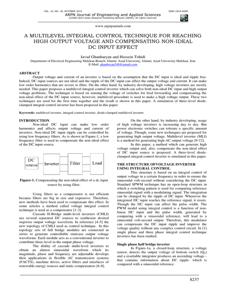
using low frequency filters. As is shown in Figure-1, a low
frequency filter is used to compensate the non-ideal effect
of the DC input source.
Figure-1. Compensating the non-ideal effect of a dc input
source by using filter.
Using filters as a compensator is not efficient
because filters are big in size and expensive. Therefore,
new methods have been used to compensate this effect. In
some articles a method called voltage integral control
technique is used as a compensator [1-3].
Cascade H-Bridge multi-level inverters (CMLI)
use several separated DC sources to synthesize desired
stepwise output voltage waveform. In reference [4-5] the
new topology of CMLI used as control technique. In this
topology sets of full bridge modules are connected in
series to generate controllable staircase output voltage
waveforms. Each module acts as a conventional inverter to
contribute three-level in the output phase voltage.
The ability of cascade multi-level inverters to
obtain an almost sinusoidal waveform which its
magnitude, phase and frequency are adjustable develops
their applications in flexible AC transmission systems
(FACTS), machine drives, active filters and interfaces of
renewable energy sources and static compensators [6-8].
On the other hand, by industry developing, usage
of high voltage inverters is increasing day to day. But
power electronic switches can tolerate a specific amount
of voltage. Though, some new techniques are proposed for
generating high output voltage. Multilevel inverter (MLI)
is a method for generating high AC output voltage [9-12].
In this paper, a method which can generate high
voltage output and, also, compensate the non-ideal effect
of DC input source is proposed. A three-level diodeclamped integral control inverter is simulated in this paper.
THE STRUCTURE OFVOLTAGE INVERTER
USING INTEGRAL CONTROL
This structure is based on an integral control of
output voltage in a certain frequency in order to ensure the
sinusoidal volt-second without considering the DC input.
Standard SPWM technique has an open-loop structure in
which a switching pattern is used for comparing reference
sinusoidal signal with a modulating signal. The integration
can be changed by the ripple of DC input. Whenever the
integrated DC input reaches the reference signal, it resets.
Though the DC input can affect the pulse width. The
PWM model using integral control is a function of nonlinear DC input and the pulse width, generated by
comparing with a sinusoidal reference, will lead to a
sinusoidal volt-second output. Therefore, this modulator
can compensate the DC input ripple and improve the
voltage quality without any complex control circuit. In [1]
single phase and three phase integral control technique
inverters has been studied.
Single phase half bridge inverter
In Figure-1a, a closed-loop structure, a voltage
sensor, detects the output voltage of bottom switch (Q2)
and a resettable integrator produces an ascending voltage that contains information about DC ripple- which is
compared with a sinusoidal reference.
8237
VOL. 10, NO. 18, OCTOBER 2015
ISSN 1819-6608
ARPN Journal of Engineering and Applied Sciences
©2006-2015 Asian Research Publishing Network (ARPN). All rights reserved.
www.arpnjournals.com
Figure-4. Voltage waveform of bottom switch (Q2).
Figure-1a. Integral control for a half-bridge single
phase inverter.
In Figure-1a it is assumed that DC input voltage
is ripple free. In order to simulate this ripple a low peak to
peak AC voltage source is used after DC input. The gating
signal of the IGBT switches, used in this circuit, is
generated by feed forwarding from the bottom switch (Q2)
voltage. This procedure is generating a gating signal that
depends on DC input voltage and its ripple, therefore nonlinear effects of DC input source will be compensated.
Gating signal circuit by integrating of the bottom switch
voltage can include the information of DC input. The
integrator used in this circuit can be reset externally and
whenever the integrated voltage of DC input reaches the
reference voltage, reset signal will be sent.
Figure-5. Gating signal of bottom switch (Q2).
Three phase inverter
In figure-6 a three-phase inverter is illustrated. In
this circuit, DC input is 70V, switching frequency is
1980Hz, reference frequency is 60Hz, Gain of voltage
sensor is 0.06 and DC offset voltage of reference is 2V
with frequency of 200Hz .
Figure-6. Three-phase inverter.
For generating the gating signal of each leg,
voltage of bottom switch in each leg is used. Line-line
voltage and line-line current waveforms of three phase
load are shown in Figure-7, Figure-8, respectively.
Figure-2. Gating signal circuit, feed forward from
the bottom switch.
In Figure-2 integrated DC input and reference
voltages are compared in a comparator, whenever these
two voltages are equal the comparator sends a signal to a
flip-flop. By receiving this signal, the S-R latch resets and
toggles the gating signal. The square voltage source
frequency is equal to the switching frequency and should
be set manually. The integrator output waveform for a half
bridge inverter is shown in Figure-3. Voltage waveform of
bottom switch (Q2) and gating signal of this switch are
illustrated in Figure-4 and Figure-5, respectively.
Figure-7. Line-line voltage of load waveform.
Figure-8. Line-line current of load waveform.
Figure-3. Integrator output waveform for single phase
half bridge inverter.
In order that the integrator works efficiently, time
constant of integrator should be less than a particular
quantity. Supposed that reference voltage and output
voltage of integrator are like below [1]:
8238
VOL. 10, NO. 18, OCTOBER 2015
ISSN 1819-6608
ARPN Journal of Engineering and Applied Sciences
©2006-2015 Asian Research Publishing Network (ARPN). All rights reserved.
www.arpnjournals.com
�
��
=��
=
+ � ∗ �� 2���
� ∗�
∗�
�
Output voltage of integrator should be always
less than reference voltage, though:
��� (� ) < ��
� ∗� ∗ �
>��
�
Therefore:
τ<
� ∗� ∗
�� +�
+�
�
Cascade H-bridge multilevel inverter
Cascaded multilevel inverters (CMI) play an
important role in recent years, especially in medium and
high voltage applications, such as high-voltage direct
current (HVDC), traction, electric power transmission
system and wind energy interconnections because of its
low witching frequencies and the capability to withstand
high voltage.
Cascade H-bridge multilevel inverter requires
less circuit parts comparison with diode-clamped
multilevel inverter or flying capacitor multilevel inverter
[4]. The number of possible output voltage levels is more
than twice the number of DC sources [13]. Levels of series
H-bridge inverters can be changed easily. But this inverter
requires more DC sources than other multilevel inverters.
In Figure-10 structure of a cascade H-bridge n-level
inverter is shown.
In this paper, the integrator time constant is
0.53ms.
The frequency spectrum of line voltage and
current of three phase load is shown in Figure-9.
Figure-9. Line-line load a) voltage and b) current
harmonic frequency spectrum.
MULTILEVEL INVERTER
Nowadays, high power inverter is needed more
than ever in industry. The concept of multilevel converters
has been introduced since 1975 [14]. Multilevel inverters
have attractive features as below:
a)
Generating voltage with very low distortion and also
reducing dv/dt stresses.
b) Drawing input current in low distortion.
c) Producing smaller common mode (CM) voltage [8].
d) Working in basic and high switching frequency [9].
On the other hand, a multilevel inverter needs lots
of switches, therefore, needs more gating signal generator
circuits than a usual inverter and it makes overall system
more complex and expensive. Multilevel inverters have
three main types which are cascade H-bridge, diodeclamped, flying capacitor.
Figure-10. Structure of a cascade H-bridge
multilevel inverter.
Diode-clamped multilevel inverter
All three phases in diode-clamped multi-level
inverter require just one DC input source, though numbers
of capacitors are reduced. The capacitors can be precharged as a group. This inverter can operate efficiently in
low switching frequency [15]. But it requires a high
number of diodes which causes problem in high-level
inverters. In Figure-11 a structure of diode-clamped
multilevel inverter is shown.
8239
VOL. 10, NO. 18, OCTOBER 2015
ISSN 1819-6608
ARPN Journal of Engineering and Applied Sciences
©2006-2015 Asian Research Publishing Network (ARPN). All rights reserved.
www.arpnjournals.com
Using diodes instead of capacitors
Using just one DC input source
Simple structure
Single phase three-level diode-clamped integral
control inverter
In Figure-11 the structure of a single phase
integral control inverter is shown. The circuit that is
shown in Figure-13 is used for generating gating signals.
Figure-11. Structure of a cascade diode-clamped
multilevel inverter.
Flying capacitor multilevel inverter
Topology of flying-capacitor multilevel inverter
is the same as diode-clamped but capacitor is used instead
of diode. The voltage of capacitors is adjustable by using
phase redundancy. This inverter can control both active
and reactive power, easily. On the other hand, the great
number of capacitors makes this inverter more complex
and expensive. Setting the capacitor voltages is not easy
and switching utilization is not efficient for real power
transmission [16-17]. In Figure-12 structure of a flyingcapacitor multilevel inverter is shown.
Figure-13. Gating signal circuit, feed forward from the
bottom switch (Q1).
In this structure AC reference source doesn’t
have any DC offset, though a square voltage source in a
twice frequency of AC reference is used to be added with
reset signal of integrator. The two AC reference voltages
are in 180ο phase difference. Output voltage of integrator
and reference voltage are shown in Figure-14. When the
reference voltage is positive the gating signal circuit
generates the gating signals for switches Q1 and Q5,
however, when it’s negative the gating signals for switches
Q2 and Q6 are generated.
Figure-12. Structure of one leg of a flying-capacitor
multilevel inverter.
THREE-LEVEL DIODE-CLAMPED INVERTER
Non-linear effect of DC input can be
compensated by voltage integral control, also, to acquire
high amount of voltage and power, multilevel inverters
can be used. In this paper, a single phase and a three phase
integral control three-level inverter have been designed.
Diode-clamped multi-levels are chosen to be used. This
type of multi-level inverter is better because of:
Figure-14. Integrator output waveform for single phase
half bridge three-level integral control inverter
Voltage of bottom switch (Q1) is supposed to be sensed.
Three phase three-level diode-clamped integral
control inverter
By using three single phase inverter and
considering 120ο phase shift in each leg, a three phase
inverter can be built. In figure-15 the structure of a three
8240
VOL. 10, NO. 18, OCTOBER 2015
ISSN 1819-6608
ARPN Journal of Engineering and Applied Sciences
©2006-2015 Asian Research Publishing Network (ARPN). All rights reserved.
www.arpnjournals.com
phase three-level diode-clamed integral control inverter is
shown.
Figure-16. Waveforms of output load a) current and b)
voltage.
Low frequency harmonics have very low
amplitude and it tends to zero in high frequency
harmonics. Frequency of switching is 8100 Hz.
Figure-15. The structure of a three phase three-level
diode-clamed integral control inverter.
Gating signal generating circuit of this three
phase inverter is the same as a single phase one (Figure13). For generating the gating signal of each leg, voltage
of bottom switch of each leg is sensed.
Gating signals of the first leg is illustrated in
Figure-15a.
CONCLUSIONS
In this paper, for compensating the effect of a
non-ideal DC input source, however, generating a high
voltage output two techniques are combined with each
other and the result showed that it can be very efficient. A
three-level diode-clamped integral control inverter has
been designed and the output voltage and current
waveform showed that the effect of DC input ripple has
been compensated, however, the output voltage increased
to a high amount of voltage by using more IGBT switches
in a diode-clamped multilevel technique. The simulation
of a single phase and three phase three-level diodeclamped integral control inverter had been performed in
this paper.
REFERENCES
[1] M. Pande, G. Joos, H. Jin, P. D. Ziogas. 1997. Output
voltage integral control technique for compensating a
non-ideal dc bus in voltage source inverters. IEEE
Trans. Power Electronics. 12(2): 302-310.
[2] M. Pande, H. Jin, G. Joos. 1997. Model Integral
Control Technique for Compensating Switch Delays
and Nonideal DC Buses in Voltage-Source Inverters.
IEEE Trans. Industrial Electronics. 44(2): 182-189.
Figure-15a. Gating signals of the first leg of a three phase
three-level integral control inverter; Q1, Q5, Q2, Q6
respectively.
If higher output voltage is needed, more levels of
proposed inverter should be used. Each switch in this
structure will tolerate a part of output voltage. In Figure16 the output voltage and current are shown.
[3] E. Cengelci, S. U. Sulistijo, B. O. Woo, P. Enjeti, R.
Teodorescu, F. Blaabjerg. 1998. A New Medium
Voltage PWM Inverter Topology for Adjustable
Speed Drives. Conference Record - IEEE Industry
Applications 33th IAS Annual Meeting. 2: 1416-1423.
[4] N. Hatano T. Ise. 2008. A Configuration and Control
Method of Cascade H-Bridge Statcom. Power and
Energy Society General Meeting, Conversion and
Delivery of Electrical Energy in the 21st century,
IEEE 2008. pp. 1-8.
8241
VOL. 10, NO. 18, OCTOBER 2015
ISSN 1819-6608
ARPN Journal of Engineering and Applied Sciences
©2006-2015 Asian Research Publishing Network (ARPN). All rights reserved.
www.arpnjournals.com
[5] J. Selvaraj, N. A. Rahim. 2009. Multilevel Inverter for
Grid-Connected PV System Employing Digital PI
Controller. IEEE Trans. Ind. Electronics. 56(1).
[6] Rodriguez J, Bernet S, Bin Wu, PonttJ. O, Kouro S.
2007.
Multilevel
Voltage-Source-Converter
Topologies for Industrial Medium- Voltage Drives.
IEEE Transactions on Industrial Electronics. 54(6):
2930-2945.
[16] Suman Debnath et al. 2012. Harmonic Elimination in
Multi-level inverter using GA and PSO: a
Comparison. IEEE Students’ Conference on
Electrical, Electronics and Computer Science.
[17] S. Du, J. Liu, and T. Liu. 2013. A new close-loop
based capacitor voltage control method for modular
multilevel converter with the switching frequency of
150 Hz. In Future Energy Electronics Conference
(IFEEC), 2013 1st International. pp. 426-430.
[7] Han B, Bae B, Baek S, Jang G. 2006. New
configuration of UPQC for medium-voltage
application. IEEE Transactions on Power Delivery.
21(3): 1438-1444.
[8] S. Mariethoz, A. Rufer. 2004. Resolution and
Efficiency Improvements for Three-Phase Cascade
Multilevel Inverters. Power Electronics Specialists
Conference, PESC 04, IEEE 35th Annual. 6: 44414446.
[9] H. Liu, L. M. Tolbert, S. Khomfoi, B. Ozpineci, Z.
Du. 2008. Hybrid Cascaded Multilevel Inverter with
PWM Control Method. Power Electronics Specialists
Conference, PESC 08, IEEE. pp. 162-166.
[10] M. S. Aspalli, A. Wamanaro. 2009. Sinusoidal Pulse
Width Modulation (SPWM) With Variable Carrier
Synchronization for Multilevel Inverter Controllers.
International Conference on Control, Automation,
Communication
and
Energy
Conservation,
INCACEC.
[11] L. M. Tolbert, F. Z. Peng, and T. Habetler. 1999.
Multilevel Converters for Large Electric drives. IEEE
Trans. Ind. Applicant. 35: 36-44.
[12] C. Hochgraf, R. Lasseter, D. Divan, T. A. Lipo. 1994.
Comparison of Multilevel Inverters for Static Var
Compensation. Conference Record - IEEE Industry
Applications Society 29th Annual Meeting. pp. 921928.
[13] J. S. Lai and F. Z. Peng. 1996. Multilevel ConvertersA new Breed of Power Converters. IEEE Trans. Ind.
Applicant. 32: 509-517.
[14] R. H. Baker and L. H. Bannister, “Electric power
converter,” U.S. Patent. 3867643, Feb. 1975.
[15] J. Rodriguez, J. S. Lai and F. Z. Peng. 2002.
Multilevel Inverters: Survey of Topologies, Controls,
and Applications. IEEE Transactions on Industry
Applications. 49(4): 724-738.
8242


