ECE380 Digital Logic Performance issues
advertisement

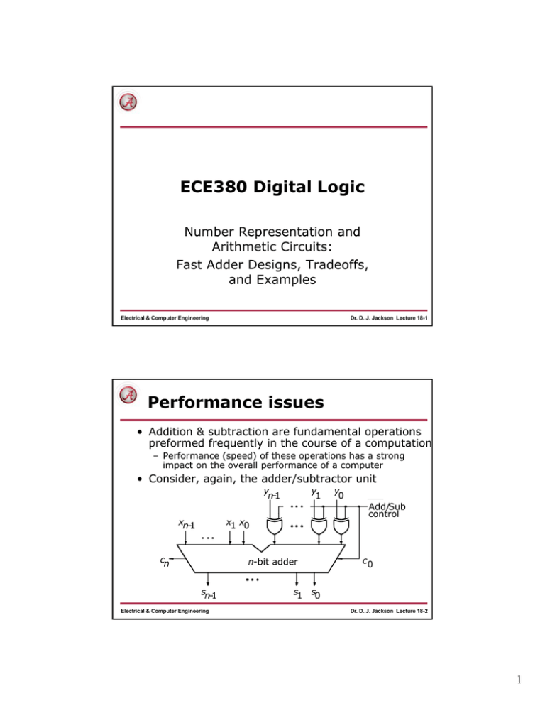
ECE380 Digital Logic Number Representation and Arithmetic Circuits: Fast Adder Designs, Tradeoffs, and Examples Electrical & Computer Engineering Dr. D. J. Jackson Lecture 18-1 Performance issues • Addition & subtraction are fundamental operations preformed frequently in the course of a computation – Performance (speed) of these operations has a strong impact on the overall performance of a computer • Consider, again, the adder/subtractor unit y n–1 xn–1 y 1 x1 x0 cn n-bit adder sn–1 Electrical & Computer Engineering y 0 Add/Sub control c0 s1 s0 Dr. D. J. Jackson Lecture 18-2 1 Adder/subtractor performance • We are interested in the largest delay from the time the operands X and Y are presented as inputs until the time all bits of the sum S and the final carry-out, cn, are valid • Assume the adder is constructed as a ripplecarry adder and that each bit in the adder is constructed as a full adder as shown xi si yi ci Electrical & Computer Engineering ci+1 Dr. D. J. Jackson Lecture 18-3 Adder/subtractor performance • The delay for the carry-out in this circuit, t, is equal to two gate delays • From the discussion of the ripple-carry adder, we know that the final result of an n-bit addition is valid after a delay of nt. This is 2n gate delays • In addition to the delay in the ripple-carry path, there is also a one gate delay introduced in the XOR gates that provide either the true or complement form of Y to the adder inputs – The total gate delay for the adder/subtractor circuit is 2n+1 • The speed of any circuit is limited by the longest delay along the paths through the circuit – The longest delay is called the critical-path-delay, and the path that causes this delay is called the critical path Electrical & Computer Engineering Dr. D. J. Jackson Lecture 18-4 2 Carry-lookahead adder • To reduce delay caused by the effect of carry propagation through the ripple-carry adder, we will attempt to evaluate quickly for each adder stage whether the carry-in from the previous stage will have a value of 0 or 1 – If we can do this quickly, we can improve the performance of the complete adder • Essentially we are attempting to reduce the critical-path-delay Electrical & Computer Engineering Dr. D. J. Jackson Lecture 18-5 Carry-lookahead adder • Recall the carry-out function for stage I can be realized as ci+1=xiyi+xici+yici ci+1=xiyi+(xi+yi)ci • Let gi=xiyi and pi=xi+yi, so ci+1= gi+pici • The function gi=1 when both xi and yi are 1, regardless of the incoming carry ci – Since in this case, stage i is guaranteed to generate a carryout, g is called the generate function • The function pi=1 when either xi and yi are 1 A carry-out is produced if ci=1 – The effect is that the carry-in of 1 is propagated through stage i; p is called the propagate function Electrical & Computer Engineering Dr. D. J. Jackson Lecture 18-6 3 Carry-lookahead (CLA) adder • Let us generate an expression for the output carry of an n-bit adder given, and, therefore, cn= gn-1+pn-1cn-1 cn-1= gn-2+pn-2cn-2 cn= gn-1+pn-1(gn-2+pn-2cn-2) cn= gn-1+pn-1gn-2+ pn-1pn-2cn-2 • The same expansion for other stages, ending with stage 0, gives cn= gn-1+pn-1gn-2+ pn-1pn-2gn-3+…+pn-1pn-2…p1g0+pn-1pn-2…p0c0 Electrical & Computer Engineering Dr. D. J. Jackson Lecture 18-7 Carry-lookahead (CLA) adder carry generated in stage n-2, and propagated through remaining stages carry generated in stage 0, and propagated through remaining stages cn= gn-1+pn-1gn-2+ pn-1pn-2gn-3+…+pn-1pn-2…p1g0+pn-1pn-2…p0c0 carry generated in last stage Electrical & Computer Engineering carry generated in stage n-3, and propagated through remaining stages Input carry c0 propagated through all stages Dr. D. J. Jackson Lecture 18-8 4 Ripple-carry adder critical path 3 gate delays for c1, 5 gate delays for c2 g c x y 1 p 1 x 1 g 1 c 2 y 0 p 0 0 0 c 1 0 Stage 1 In general, 2n+1 delays s for n-bit ripple-carry adder 1 Stage 0 Electrical & Computer Engineering Dr. D. J. Jackson Lecture 18-9 s 0 Carry-lookahead critical path x 3 gate delays for c1, 3 gate delays for c2 3 gate delays for cn y 1 x0 g 1 g 0 p 1 c 2 Total delay for n-bit CLA adder is 4 gate delays All gi and pi, one delay All ci, two more delays One more delay for the sums si Electrical & Computer Engineering x 1 c s 1 0 y 0 y0 p 0 c 0 1 s 0 Dr. D. J. Jackson Lecture 18-10 5 Carry-lookahead limitations • The expression for carry in a CLA adder cn= gn-1+pn-1gn-2+ pn-1pn-2gn-3+…+pn-1pn-2…p1g0+pn-1pn-2…p0c0 • obviously results in a fast solution (since it is only a 2 level AND-OR function) • Fan-in limitations may effectively limit the speed of a CLA adder – Devices with known fan-in limitations (such as an FPGA) often include dedicated circuitry for implementation of fast adders • The complexity of an n-bit CLA adder increases rapidly as n becomes large – To reduce this complexity, we can use a hierarchical approach in designing large adders Electrical & Computer Engineering Dr. D. J. Jackson Lecture 18-11 32-bit adder design • Suppose we want to design a 32-bit adder • Divide this adder into 4 blocks such that – – – – Bits Bits Bits Bits b7-0 are block 0 b15-8 are block 1 b23-16 are block 2 b31-24 are block 3 • Each block can be constructed as an 8-bit CLA adder – The carry-out signals from the four blocks are c8, c16, c24, and c32 • There are 2 basic approaches for interconnecting these four blocks – Ripple-carry between blocks – Second level carry-lookahead circuit Electrical & Computer Engineering Dr. D. J. Jackson Lecture 18-12 6 Ripple-carry between blocks X24-31 Y24-31 C32 X16-23 Y16-23 C24 Block 3 S24-31 Block 2 X8-15 Y8-15 C16 X7-0 Y7-0 C8 Block 1 S16-23 Block 0 S8-15 C0 S7-0 Electrical & Computer Engineering Dr. D. J. Jackson Lecture 18-13 Second level carry-lookahead circuit x y 31-24 31-24 Block 3 G P 3 3 c x y 15-8 15-8 Block 1 c24 s G P 11 31-24 32 x c 16 y 7-0 7-0 Block 0 G P 00 s15-8 c c 0 s 7–0 8 Second-level lookahead Electrical & Computer Engineering Dr. D. J. Jackson Lecture 18-14 7 Second level carry-lookahead circuit • For the second level circuit: P0=p7p6p5p4p3p2p1p0 G0=g7+p7g6+p7p6g5+…+p7p6p5p4p3p2p1g0 c8=G0+P0c0 c16= G1+P1c8= G1+P1G0+P1P0c0 c24= G2+P2G1+P2P1G0+P2P1P0c0 c32= G3+P3G2+P3P2G1+P3P2P1G0+P3P2P1P0c0 Electrical & Computer Engineering Dr. D. J. Jackson Lecture 18-15 Hierarchical CLA analysis • Assuming a fan-in constraint of four inputs, the time to add two 32-bit numbers involves – five gate delays to develop the Gi and Pi terms, three gate delays for the second-level lookahead, and one delay (XOR) to produce the final sum bits. – Actually the final sum bit is computed after eight delays because c32 is not used to determine the sum bits. – The complete operation, including overflow detection (c31c32) takes nine gate delays (compared to 65 for the ripple carry adder) Electrical & Computer Engineering Dr. D. J. Jackson Lecture 18-16 8


