ODIN MIT4 02
Fiber Optic Transmitter for MOST®
Data Sheet
Description
Features
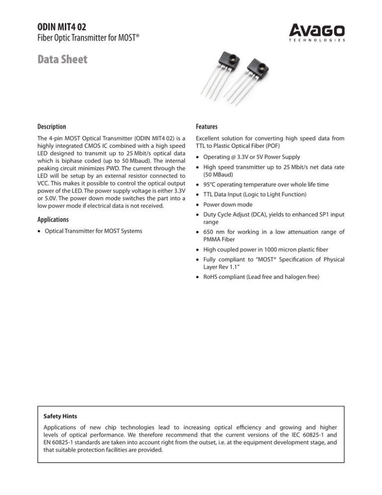
The 4-pin MOST Optical Transmitter (ODIN MIT4 02) is a
highly integrated CMOS IC combined with a high speed
LED designed to transmit up to 25 Mbit/s optical data
which is biphase coded (up to 50 Mbaud). The internal
peaking circuit minimizes PWD. The current through the
LED will be setup by an external resistor connected to
VCC. This makes it possible to control the optical output
power of the LED. The power supply voltage is either 3.3V
or 5.0V. The power down mode switches the part into a
low power mode if electrical data is not received.
Excellent solution for converting high speed data from
TTL to Plastic Optical Fiber (POF)
Applications
• Optical Transmitter for MOST Systems
• Operating @ 3.3V or 5V Power Supply
• High speed transmitter up to 25 Mbit/s net data rate
(50 MBaud)
• 95°C operating temperature over whole life time
• TTL Data Input (Logic to Light Function)
• Power down mode
• Duty Cycle Adjust (DCA), yields to enhanced SP1 input
range
• 650 nm for working in a low attenuation range of
PMMA Fiber
• High coupled power in 1000 micron plastic fiber
• Fully compliant to “MOST® Specification of Physical
Layer Rev 1.1”
• RoHS compliant (Lead free and halogen free)
Safety Hints
Applications of new chip technologies lead to increasing optical efficiency and growing and higher
levels of optical performance. We therefore recommend that the current versions of the IEC 60825-1 and
EN 60825-1 standards are taken into account right from the outset, i.e. at the equipment development stage, and
that suitable protection facilities are provided.
Table 1. Absolute Maximum Ratings Limit Values
Parameter
Symbol
min.
max
Unit.
Supply Voltage
VCCMax
-0.5
6.0
V
Storage Temperature Range
TSTG
-40
100
°C
Soldering Temperature (>2.5 mm from case bottom t ≤ 10s)
TS
–
260
°C
-0.5
VCC +0.5
V
–
2.0
kV
Voltage at any PIN
Electrostatic Discharge Voltage Capability[1]
ESD
Notes:
1. ESD Capability for all Pins HBM (human body model) according JESD22-A114B.
Table 2. Recommended Operating Conditions
Limit Values
Parameter
Symbol
min.
max.
Unit
Supply Voltage low
VCC_l
3.135
3.465
V
Supply Voltage high
VCC_h
4.75
5.25
V
Operating Temperature Range (ambient)[1]
TA
-40
95
°C
Notes:
1. For details see application note “Handling, Storage, Operating and Processing Application Note of ODIN MOST4 Transceiver”
All the data in this specification refers to the operating conditions above and over life time unless otherwise stated.
Table 3. DC Characteristics Limit Values
Parameter
Symbol
min.
typ.
max.
Unit
Low Level Input Voltage
VIL
-0.3
–
0.8
V
High Level Input Voltage
VIH
2.0
–
VCC + 0.3
V
Input Leakage Current(VCC = 5.0 V, VI = 0.0 V or VI = 5.0 V)
IL
–
–
± 20
µA
Input Capacitance
CI
–
–
7
pF
Input Resistance
RI
2
–
–
kΩ
Supply Current (Rext = 15 kΩ) ON state, biphase coded data[1]
ICC
–
–
35
mA
Supply Current (Rext = 15 kΩ) OFF state[2]
ILP2
–
–
20
µA
Notes:
1. The current through the LED and therefore the optical output power and overall power consumption depends on the settings of Rext. The
nominal value for Rext is 15 kΩ. With Rext = 30 kΩ the optical output power is about -3 dB of the nominal value. Typical behavior see Figure 1.
Important: The external resistor of Rext must be within the range of 13.5 kΩ to 33 kΩ. For values of Rext out of this range functionality
may not be given over the whole temperature range and the device lifetime. Using values below 13 kΩ for Rext can damage the
transmitter.
2. If the transmitter is in full power mode it is switched OFF 1 ms (max.) after TX DATA is low. If the transmitter is in low power mode it is switched
ON 6 ms (max.) after TX DATA transmission starts.
Attention
Stresses above those listed here may cause permanent damage to the device. Exposure to absolute maximum
rating conditions for extended periods may affect device reliability. Between 3.465V and 4.75V the device is not
specified according Table2. Therefore operation is limited to the range of 3.135V ... 3.465V or 4.75V ... 5.25V.
Table 4.1 AC Electrical Characteristics 45Mbaud (44.1kHz)
Limit Values
Parameter
Symbol
min.
typ.
max.
Unit
Test Conditions
Power Up Time
TPU
–
0.016
6
ms
Zero -->MOST
DataPower Down Time
TPD
–
0.01
1.0
ms
MOST Data -->Zero
Optical Signal Characteristics (22.5 Mbit MOST Data, VCC = 3.135 ... 3.465 V or 4.75 … 5.25 V, Rext = 15 kOhm)
Limit Values
Parameter
Symbol
min.
typ.
max.
Unit
Peak wavelength
λPeak
630
650
685
nm
Temperature coefficient λPeak
TCλ
–
0.16
–
nm/K
Spectral bandwidth (FWHM)
Deltaλ
–
20
30
nm
Average Output Power coupled into plastic fiber [1]
Popt
-9.0
-5.2
-2.0
dBm
Average Output Power coupled into plastic fiber
(if Rext = 13.5k is used instead of Rext = 15k)[1]
Popt
-8.5
-4.7
-1.5
dBm
Optical Output Power “Light off“[2]
Poff
–
-50
dBm
Optical Rise Time (20% - 80%)[4]
tr
–
2.5
6
ns
Optical Fall Time (20% - 80%)[4]
tf
–
3.5
6
ns
Extinction Ratio[4][6]
re
10
12
–
dB
Pulse Width Variation [3][4][5]
tPWV
20.0
–
24.3
ns
Average Pulse Width Distortion[3][4]
tAPWD
-1.4
–
1.4
ns
Data Dependent Link Jitter[3][4]
tDDJ
–
0.20
0.77
ns
Uncorrelated Link Jitter[3][4]
tUJ
–
0.05
0.33
ns
Positive Overshoot within 0UI..2/3UI[4][6]
-20
–
40
%
Negative Overshoot within –1UI..–1/4UI[4][6]
-10
–
20
%
High Level Signal Ripple between 2/3UI and 3/4UI[4][6]
-10
–
10
%
Notes:
1. Average value, when transmitting modulated light @ signal timing paramters. The output power coupled into plastic fiber Popt is measured with
a large area detector at the end of 30 cm POF fiber with a NA = 0.5, which is ideally coupled to the transmitter.
2. Average value, when signal on Tx_Data is low.
3. The electrical input signal has to fulfill following requirements: tPWV(min) = 20.1 ns, tPWV(max) = 24.1 ns, tAPWD(min) = -1.5 ns and tAPWD(max) = 1.5 ns,
tDDJ(max).= 0.22 ns, tUJ(max).= 0.10 ns.
4. Characterized with Avago Characterization Boards as described in the Application note “Application Note MOST circuit for Avago ODIN
Transceiver“.
5. Limits for 2UI are 42.2 ... 46.4ns and for 3UI thay are 64.3 ... 68.5ns.
6. Top and Base level measured at least over 10UIs.
Table 4.2 Electrical Characteristics 49.152MBaud (48kHz)
Limit Values
Parameter
Symbol
min.
typ.
max.
Unit
Test Conditions
Power Up Time
TPU
–
0.016
6
ms
Zero -->MOST
DataPower Down Time
TPD
–
0.01
1.0
ms
MOST Data -->Zero
Optical Signal Characteristics (24.576 Mbit MOST Data, VCC = 3.135 ... 3.465 V or 4.75 … 5.25 V, Rext = 15 kOhm)
Limit Values
Parameter
Symbol
min.
typ.
max.
Unit
Peak wavelength
λPeak
630
650
685
nm
Temperature coefficient λPeak
TCλ
–
0.16
–
nm/K
Spectral bandwidth (FWHM)
Deltaλ
–
20
30
nm
Average Output Power coupled into plastic fiber [1]
Popt
-9.0
-5.2
-2.0
dBm
Average Output Power coupled into plastic fiber
(if Rext = 13.5k is used instead of Rext = 15k)[1]
Popt
-8.5
-4.7
-1.5
dBm
Optical Output Power “Light off“[2]
Poff
–
-50
dBm
Optical Rise Time (20% - 80%)[4]
tr
–
2.5
5.5
ns
Optical Fall Time (20% - 80%)[4]
tf
–
3.5
5.5
ns
Extinction Ratio[4][6]
re
10
12
–
dB
Pulse Width Variation [3][4][5]
tPWV
18.4
–
22.3
ns
Average Pulse Width Distortion[3][4]
tAPWD
-1.3
–
1.3
ns
Data Dependent Link Jitter[3][4]
tDDJ
–
0.20
0.71
ns
Uncorrelated Link Jitter[3][4]
tUJ
–
0.05
0.31
ns
Positive Overshoot within 0UI..2/3UI[4][6]
-20
–
40
%
Negative Overshoot within –1UI..–1/4UI[4][6]
-10
–
20
%
High Level Signal Ripple between 2/3UI and 3/4UI[4][6]
-10
–
10
%
Notes:
1. Average value, when transmitting modulated light @ signal timing paramters. The output power coupled into plastic fiber Popt is measured with
a large area detector at the end of 30 cm POF fiber with a NA = 0.5, which is ideally coupled to the transmitter.
2. Average value, when signal on Tx_Data is low.
3. The electrical input signal has to fulfill following requirements: tPWV(min) = 18.4ns tpwv(max) = 22.3ns, tAPWD(min) = -1.3ns and tAPWD(max) = 1.3ns,
tDDJ(max) = 0.20ns and tUJ = 0.09ns.
4. Characterized with Avago Characterization Boards as described in the Application note “Application Note MOST circuit for Avago ODIN
Transceiver“
5. Limits for 2UI are 38.72 … 42.66ns and for 3UI are 59.06 … 63.01ns
6. Top and Base level measured at least over 10UIs
35
140
Range for Rext = 13.5 … 33 kOhm
30
100
80
25
60
40
Current [mA]
Average Optical Output Power [%]
120
20
20
0
10
13.5
15
20
25
30
33
15
35
External Resistor Rext [kOhm]
Figure 1. Typical Dependency of Average Optical Output Power Popt and Supply Current versus External Resistor Rext (22.5 Mbit MOST Data,
VCC = 5.0 V, TA = 25 °C)
Popt [%]
Icc [mA]
Package Outlines
ODIN MIT4 02(Cavity as Interface Package)
Dimensions in mm
For a more detailed drawing please contact Avago Technologies.
Disclaimer
The information herein is given to describe certain components and shall not be considered as a guarantee of
characteristics.
Terms of delivery and rights to technical change reserved.We hereby disclaim any and all warranties, including but
not limited to warranties of non-infringement, regarding circuits, descriptions and charts stated herein.
Warnings
Due to technical requirements components may contain dangerous substances. For information on the types inquestion please contact your nearest Avago Technologies Office.
Avago Technologies Components may only be used in life-support devices or systems with the express written
approval of Avago Technologies, if a failure of such components can reasonably be expected to cause the failure
of that life-support device or system, or to affect the safety or effectiveness of that device or system. Life support
devices or systems are intended to be implanted in the human body, or to support and/or maintain and sustainand/or protect human life. If they fail, it is reasonable to assume that the health of the user or other persons
maybe endangered.
Information
For further information on technology, delivery terms and conditions and prices please contact your nearest
Avago Technologies Office (www.avagotech.com).
Revision History
Current Document:
AV02-0747EN - November 5, 2007
Previous Version:
AV02-0747EN - October 3, 2007
Page
Subjects (major changes since last revision)
3, 4
Rounding of numbers
7
Addition of “Revision History”
For product information and a complete list of distributors, please go to our web site:
www.avagotech.com
Avago, Avago Technologies, and the A logo are trademarks of Avago Technologies, Limited in the United States and other countries.
Data subject to change. Copyright © 2007 Avago Technologies Limited. All rights reserved.
AV02-0747EN - November 5, 2007
