International Journal of Science, Engineering and Technology Research (IJSETR), Volume 3, Issue 5, May 2014
A Single-Phase Carrier Phase-shifted PWM
Multilevel Inverter for 9-level with Reduced
Switching Devices
Ravi Yadav, Praveen Bansal
Abstract— This paper proposes a new multi-level inverter
topology is called Reversing Voltage that utilizes less number of
switches than conventional topology and it shows the
comparison between different level in single-phase. A
multilevel inverter is a power electronic device that is used for
high voltage and high power applications such as flexible AC
transmission systems, uninterruptible power supplies and PV
systems and their performance is better to that of conventional
two-level inverters due to higher number of dc voltage sources,
reduced harmonic distortion and lower EMI. A Carrier
phase-sifted PWM technique is used for the proposed
multilevel inverter because it offers great advantages such as is
improved output voltage waveforms, minimize total harmonic
distortion, and control EMI when compared with other PWM
techniques. A proposed multi-level inverter topology is used to
generate 9-level output voltage in single-phase and the same is
to be simulated with the different PWM techniques and its
effect on the harmonic spectrum is calculated. The system is
design with the help of MATLAB/SIMULINK.
inverter offers several advantages over two-level inverter
hence improves the output voltage waveform, reduced (dv/dt)
voltage stress on the load and also reduces electromagnetic
interference problems, but it has some disadvantages. One of
the most obvious disadvantages is the requirement of higher
number of power semiconductor switches. Every switch
requires a gate driver circuit, therefore increasing the
complexity and size of the overall circuit [4]. Lower voltage
rated switches can be used in multi-level inverter instead of
higher number of semiconductor switches which can be
minimized cost of the semiconductor switches as compared
to two level inverter.
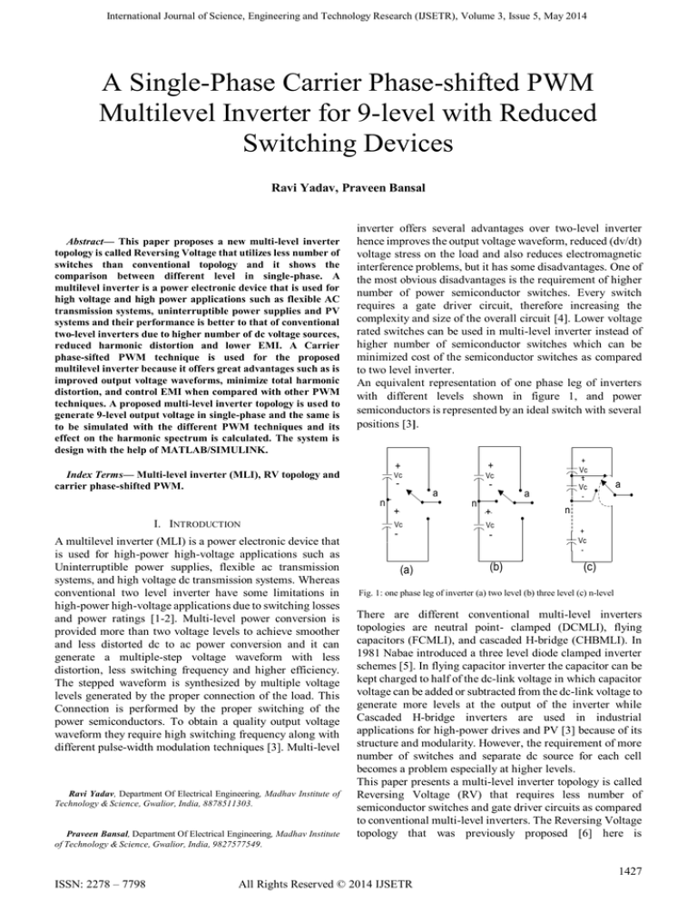
An equivalent representation of one phase leg of inverters
with different levels shown in figure 1, and power
semiconductors is represented by an ideal switch with several
positions [3].
Vc
-
n
I. INTRODUCTION
A multilevel inverter (MLI) is a power electronic device that
is used for high-power high-voltage applications such as
Uninterruptible power supplies, flexible ac transmission
systems, and high voltage dc transmission systems. Whereas
conventional two level inverter have some limitations in
high-power high-voltage applications due to switching losses
and power ratings [1-2]. Multi-level power conversion is
provided more than two voltage levels to achieve smoother
and less distorted dc to ac power conversion and it can
generate a multiple-step voltage waveform with less
distortion, less switching frequency and higher efficiency.
The stepped waveform is synthesized by multiple voltage
levels generated by the proper connection of the load. This
Connection is performed by the proper switching of the
power semiconductors. To obtain a quality output voltage
waveform they require high switching frequency along with
different pulse-width modulation techniques [3]. Multi-level
Ravi Yadav, Department Of Electrical Engineering, Madhav Institute of
Technology & Science, Gwalior, India, 8878511303.
Praveen Bansal, Department Of Electrical Engineering, Madhav Institute
of Technology & Science, Gwalior, India, 9827577549.
Vc
a
+
Vc
-
(a)
+
Vc
+Vc
-
+
+
Index Terms— Multi-level inverter (MLI), RV topology and
carrier phase-shifted PWM.
-
n
+
Vc
-
(b)
a
a
n
+
Vc
-
(c)
Fig. 1: one phase leg of inverter (a) two level (b) three level (c) n-level
There are different conventional multi-level inverters
topologies are neutral point- clamped (DCMLI), flying
capacitors (FCMLI), and cascaded H-bridge (CHBMLI). In
1981 Nabae introduced a three level diode clamped inverter
schemes [5]. In flying capacitor inverter the capacitor can be
kept charged to half of the dc-link voltage in which capacitor
voltage can be added or subtracted from the dc-link voltage to
generate more levels at the output of the inverter while
Cascaded H-bridge inverters are used in industrial
applications for high-power drives and PV [3] because of its
structure and modularity. However, the requirement of more
number of switches and separate dc source for each cell
becomes a problem especially at higher levels.
This paper presents a multi-level inverter topology is called
Reversing Voltage (RV) that requires less number of
semiconductor switches and gate driver circuits as compared
to conventional multi-level inverters. The Reversing Voltage
topology that was previously proposed [6] here is
1427
ISSN: 2278 – 7798
All Rights Reserved © 2014 IJSETR
International Journal of Science, Engineering and Technology Research (IJSETR), Volume 3, Issue 5, May 2014
implemented in single-phase nine-level inverter with carrier
phase-shifted PWM technique. A Carrier phase-shifted
PWM technique offers great advantages such as improved
output voltage waveforms, lower EMI, and lower THD in
comparison of other PWM techniques.
The block diagram of multi-level inverter using Reversing
Voltage topology is shown in fig. 2.1. The principle idea is
that, the left side circuit in fig. 2.2 generates the required
positive level is called positive level generator of fig. 2.1 and
the right side circuit of fig. 2.2 is called full bridge converter
of fig.2.1 which reverses the voltage direction when the
voltage polarity requires to be changed for negative polarity
(negative half cycle of the fundamental output voltage) [6].
Positive level
Generator
Full bridge
converter
s1
Vdc
II. PROPOSED TOPOLOGY
DC Power
supply
The operation of the proposed topology has been discussed
in detail and has been verified with the help of simulations.
Load
s7
s2
s3
Vdc
1
s9
s11
output
s8
s4
s10
s12
Vdc
2
s5
Vdc
s6
Fig. 2.2 Proposed single-phase 9-level inverter using RV topology.
PWM
Controller
Fig. 2.1 Block diagram of multi-level inverter using Reversing Voltage
topology.
This Reversing Voltage topology requires twelve
semiconductor switches and four isolated dc sources shown
in fig 2.2 which separates in two parts. One part is called
level generation part (left side) and is responsible for level
generating in positive polarity. The other part is called
polarity generation part (right side) and is responsible for
generating the polarity of the output voltage. This topology
combines the two parts (left part and right part) to generate
the multi-level output voltage waveform. The positive level
are generated by the left part (level generation), and then,
this part is fed to a full-bridge inverter (polarity generation),
which will generate the required polarity for the output. The
proposed topology is a symmetrical topology since all the
values of all voltage sources are equal and it does not face
voltage-balancing problems due to fixed dc voltage values
[7].
The primary objective of this paper is to minimize the total
harmonic distortion of 9-level inverter with carrier phase
shifted PWM technique using Reversing Voltage topology
and it shows the comparison between different level. It also
minimizes power semiconductor switches than conventional
multilevel inverter.
A. Operation of a Single-Phase 9-Level Inverter Using
Reversing Voltage TopologyOperation of the single-phase 9-level MLI with reversing
voltage topology can be easily explained with the help of fig.
2.2 and table I. When switches S2, S4, S5 and S7 are turned
“on” the output voltage will be “Vdc” (i.e., level 1). The
output voltage will be “2Vdc” (i.e., level 2) when switches
S2, S5, S7 and S8 are turned “on”. When S2, S6 and S7
switches are turned “on” the output voltage will be “3Vdc”
(i.e., level 3). When switches S1 and S6 are turned on the
output voltage will be “4Vdc” (i.e., level 4). When switches
S2, S3, S4 and S5 are turned “on” the output voltage is zero
(i.e., level 0). Switches S9, S10, S11 and S12 are used for a
complementary pair. When S10 and S11 are turned “on”
together, positive half cycle can be generated and when S9
and S12 are turned “on” together, negative half cycle can be
generated across load. The voltage blocking capacity of each
switch is Vdc [2].
The operation of this topology can also be easily
understood by mode of operation of single-phase nine-level
inverter shown in figure 2.3. Each voltage source “Vdc” is
required 100V. There are nine sufficient switching modes in
generating the multistep level for a 9-level multilevel
inverter.
According to the table, there are nine switching
combinations to control the MLI and it shows the great
redundancy of this topology.
For a conventional single-phase 9-level MLI model, it uses
16 switches, whereas the proposed model uses only 12
switches.
[8].
TABLE-I
1428
ISSN: 2278 – 7798
All Rights Reserved © 2014 IJSETR
International Journal of Science, Engineering and Technology Research (IJSETR), Volume 3, Issue 5, May 2014
GENERATION
OF LEVEL
SWITCH STATES
S1
S2
S3
S4
S5
4
S7
S8
S9
3
2
1
0
-1
-2
-3
-4
S6
S12
OUTPUT
VOLTAGE
S10
S11
4Vdc
3Vdc
2Vdc
Vdc
0
-Vdc
-2Vdc
-3Vdc
- 4Vdc
B. MODE OF OPERATION
s1
s1
Vdc
Vdc
s7
s7
s2
s2
1
s3
Vdc
s9
-
s4
s8
s3
Vdc
Vo +
Load
s10
s4
s8
- Vo +
s10
Vdc
s11
s12
2
Vdc
s5
2
s5
Vdc
s6
Vdc
s6
Level
Level-0
-1
Fig. (c)
Fig. (a)
s1
s1
Vdc
s9
Load
s11
s12
1
Vdc
s7
s7
s2
s2
1
1
s3
s3
Vdc
s4
s8
Vdc
s9
s11
s10
s12
-
Vo +
Load
s9
s11
s10
s12
-
Vdc
s8
s4
Vdc
Vo +
Load
2
2
s5
s5
Vdc
Vdc
s6
s6
Level
+1
Fig. (b)
Level +2
Fig. (d)
1429
ISSN: 2278 – 7798
All Rights Reserved © 2014 IJSETR
International Journal of Science, Engineering and Technology Research (IJSETR), Volume 3, Issue 5, May 2014
s1
Vdc
s7
s1
Vdc
s2
s7
s2
1
s3
Vdc
1
s9
s11
- Vo +
s3
Vdc
s4
s10
S12
s11
s10
s12
-
Load
s8
s9
s4
s8
Vo +
Load
Vdc
Vdc
2
2
s5
s5
Vdc
Vdc
s6
s6
Level +4
Level - 2
Fig.(h)
Fig. (e)
s1
s1
Vdc
s7
Vdc
s2
s3
Vdc
s2
s4
Vdc
1
s9
-
s8
s7
1
s3
s11
Vo +
Load
Vdc
- Vo +
s12
s4
s8
2
Vdc
s6
s6
Level +3
Fig. (f)
Level - 4
Fig. (i)
Fig. 2.3: Fig (a), Fig (b), Fig (c), Fig (d), Fig (e), Fig. (f), Fig. (g), Fig. (h), Fig.
(i) are Switching combinations of 9-level multi-level inverter topology.
s1
s2
III. MODULATION TECHNIQUES
1
s3
Vdc
s9
- Vo +
s11
Load
s4
s10
S12
Vdc
s5
Vdc
s6
Level -3
Fig. (g)
S12
s5
Vdc
s8
s10
Vdc
2
s7
s11
Load
s10
s5
Vdc
s9
2
There are different pulse width modulation strategies with
different phase relationships.
a. Phase disposition pulse width modulation (PD PWM):- In
phase disposition pulse width modulation strategy,
where all carrier waveforms are in same phase.
b. Phase opposition disposition pulse width modulation
(POD PWM):- In phase opposition disposition pulse
width modulation strategy, where all carrier waveforms
above zero reference are in phase and below zero
reference are 1800 out of phase.
c. Alternate phase opposition disposition pulse width
modulation (APOD PWM):- In alternate phase
opposition disposition PWM scheme where every carrier
waveform
is in out of phase with its neighbor carrier by
0
180 .
d. Phase-shifted pulse width modulation (PS PWM):Fig.3.1 shows the carrier Phase-shifted pulse width
modulation strategy. A carrier phase shifted PWM for
multi-level inverter is used to generate the stepped
1430
ISSN: 2278 – 7798
All Rights Reserved © 2014 IJSETR
International Journal of Science, Engineering and Technology Research (IJSETR), Volume 3, Issue 5, May 2014
multi-level output voltage waveform with lower % THD.
In proposed, before implementing the Multicarrier
PWM Techniques, the gating signals of multi-level
inverter switches are generated by comparing sinusoidal
reference wave with triangular carrier waves (N-1=3)
with 1200 phase displacement and a constant value at
specific intervals of time producing the characteristic
multistep output waveform. MLI with N levels requires
(N-1) triangular carriers. In phase shifted PWM, all the
triangular carriers have same frequency and same peak
to peak amplitude [9].
TABLE-II
PERCENTAGE THD COMPARISON FOR DIFFERENT LEVEL
MODULATION
PS PWM %THD
PS PWM %THD
INDEX
FOR 9-LEVEL
FOR 7-LEVEL
4
1.1
12.65
17.77
1
13.90
18.68
0.9
14.49
19.96
0.8
15.93
21.91
0.7
16.12
23.06
3
Selected signal: 4 cycles. FFT window (in red): 3 cycles
2
400
1
200
0
0
-1
-200
-2
-400
0
0.01
0.02
0.03
0
0.002
0.004
0.006
0.008
0.01
0.012
0.014
0.016
0.018
0.02
Time(s)
400
300
Output Voltage
200
100
0
Mag (% of Fundamental)
-4
0.04
0.05
0.06
0.07
0.08
Time (s)
-3
Fundamental (50Hz) = 389.4 , THD= 14.49%
0.6
0.4
0.2
0
0
100
200
300
400
500
600
700
800
900
1000
Frequency (Hz)
-100
Fig. 4.2: Harmonic of the output phase voltage by PSPWM for R-L load (Ma =
0.9 Mf = 20) for 9-level.
-200
Selected signal: 4 cycles. FFT window (in red): 3 cycles
-300
200
-400
0
0.002
0.004
0.006
0.008
0.01
Time(s)
0.012
0.014
0.016
0.018
0
0.02
Fig. 3.1: Carrier phase-shifted PWM technique and output voltage.
-200
IV. SIMULATION RESULTS
Mag (% of Fundamental)
In this topology, a carrier based phase shifted PWM
technique is used. The figure 2.2 shows the simulated model
of single-phase 9-level reversing voltage MLI. Twelve
IGBTs are used and each of the switches requires a separate
gate driver circuit. The simulation parameters are as
following R = 10 ohms, L = 10mH, and dc source voltage is
400V; Frequency of carrier signal is 1 kHz. Based on the
PWM techniques, the harmonic spectrum was analysed using
the FFT Window in MATLAB/Simulink. Table II shows
THD comparison between different levels. When modulation
Index is more than 1, it is called as over modulation and if it’s
below 1 called under modulation [10].
0
0.01
0.02
0.03
0.04
0.05
0.06
0.07
0.08
Time (s)
Fundamental (50Hz) = 289.8 , THD= 19.96%
1
0.5
0
0
100
200
300
400
500
600
700
800
900 1000
Frequency (Hz)
Fig. 4.2: Harmonic of the output phase voltage by PSPWM for R-L load (Ma =
0.9 Mf = 20) for 7-level.
1431
ISSN: 2278 – 7798
All Rights Reserved © 2014 IJSETR
International Journal of Science, Engineering and Technology Research (IJSETR), Volume 3, Issue 5, May 2014
The number of required components for single-phase 9-level
MLI is shown in Table III
TABLE-III
Comparison between different multilevel inverter topologies
Inverter type
Main switches
Main diodes
Clamping
diodes
DC bus
Capacitor/
Isolated
supplies
Flying
capacitors
Total numbers
NPC
Flying
capacitor
2(N-1)
2(N-1)
2(N-1)
(N-1)+4
2(N-1)
2(N-1)
2(N-1)
(N-1)+4
2(N-2)(N-1)
0
(N-1)
(N-1)(2N+1)
(N-1)(N+8)/2
REFERENCES
[1]
0
3(N-1)/2
(N-1)/2
0
0
(N-1)(N-2)/2
The authors sincerely acknowledge the Director, MITS,
Gwalior, India to carry out this work.
Proposed
0
(N-1)
0
cascade
ACKNOWLEDGMENT
11/2(N-1)
(5N+11)/2
It can be shows that the number of components of the
proposed topology is lower than that of other topologies so as
the voltage level increases the number of components will
decreases particularly for higher voltage level [7].
400
300
Phase Voltage
200
100
0
-100
-200
-300
-400
0
0.01
0.02
0.03
0.04
0.05
0.06
0.07
0.08
Time(s)
Fig. 4.3 Output phase voltage of single-phase 9-level MLI
S. Daher, J. Schmid, and F. L. M. Antunes, “Multilevel inverter
topologies for stand-alone PV systems,” IEEE Trans. Ind. Electron.,
vol. 55, no. 7, pp. 2703–2712, Jul. 2008.
[2] Hemant Joshi, P. N. Tekwani and Amar Hinduja Kolorrol
“Multilevel Inverter For Induction Motor Drives Using RV
Topology,” IEEE Trans. Ind. 2010.
[3] Jose Rodriguez, Jih-Sheng Lai and Fang Zheng Peng. “Multilevel
Inverters: A survey of topologies, controls and applications.” IEEE
Trans. Ind.Electronics.vol-49 no.4 pp 724-738, Aug. 2002.
[4] K. Jang-Hwan, S.-K. Sul, and P. N. Enjeti, “A carrier-based PWM
method with optimal switching sequence for a multilevel four-leg
voltage source inverter,” IEEE Trans. Ind. Appl., vol. 44, no. 4, pp.
1239–1248, Jul./Aug. 2008.
[5] Nabe, I. Takahashi and H. Akagi. “A new neutral point clamped
PWM inverter.” IEEE Trans. Ind. Applicat. Vol. 1A-17, pp 518523, sep. /oct. 1981.
[6] E.Najafi, A.H.M.Yatim and A.S. Samosir. “A new
topology-reversing voltage (RV) for multi-level inverters.” 2nd
International conference on power and energy (PECon 08), pp
604-608, December 2008 Malaysia.
[7] Ehsan Najafi, and Abdul Halim Mohamed Yatim, “Design and
Implementation of a New Multilevel Inverter Topology,” IEEE
Transactions on industrial electronics, vol. 59, no. 11, November
2012.
[8] Jacob James Nedumgatt, Vijayakumar D., A. Kirubakaran,
Umashankar S. “A Multilevel Inverter with Reduced Number of
Switches,” IEEE Students’ Conference on Electrical, Electronics
and Computer Science 2012.
[9] Napaphat Lekgamheng and Yuttana Kumsuwan “Phase-Shifted
PWM Stretegy of a Seven-level Single-Phase Current Source
Inverter For Grid-Connectio Systems,” IEEE Trans. Ind. Appl. vol.
978-1-4673-1792-4/13 2013.
[10] P.Palanivel Subhransu SekherDash “Phase Shifted Carrier Pulse
Width Modulation for Three Phase Multilevel Inverter to Minimize
THD and Enhance Output Voltage Performance” Copyright © JES
2010 on-line: journal.esrgroups.org/jes.
300
Phase Voltage
200
100
0
-100
-200
-300
0
0.01
0.02
0.03
0.04
0.05
0.06
0.07
0.08
Time(S)
Fig. 4.4 Output phase voltage of single-phase 7-level MLI
V. CONCLUSION
In this paper, a new multi-level inverter topology with carrier
phase-shifted pulse width modulation is proposed. Proposed
topology with carrier phase-shifted PWM technique is used
to minimize total harmonic distortion as compared to other
PWM techniques. This multi-level inverter topology
improves output voltage, reduces higher number of
semiconductor switches and voltage stress on
semiconductors switches. One of the most advantages of the
topology is that as the number of voltage level increases, the
THD is reduced especially at higher level. Simulation results
show the performance of single-phase 9-level MLI with
improved THD.
1432
ISSN: 2278 – 7798
All Rights Reserved © 2014 IJSETR
International Journal of Science, Engineering and Technology Research (IJSETR), Volume 3, Issue 5, May 2014
First Author
Ravi Yadav was born on June 12, 1990. His graduation in Electrical
Engineering from the Institute of Information Technology & Management
(IITM) in Gwalior and pursuing M.E at Madhav Institute of Technology and
Science (MITS) in Gwalior.
Second Author
Praveen Bansal obtained his bachelor of Engineering (Hon’s) in Electrical
Engineering from Madhav Institute of Technology and Science(MITS)
,Gwalior in 2009,MTech degree in Electrical Drives from Maulana Azad
National Institute of Technology in 2012,Currently he is an Assistant Professor
at MITS, Gwalior. His area of interests includes multilevel Inverters, Induction
motor modelling, and PWM techniques.
1433
ISSN: 2278 – 7798
All Rights Reserved © 2014 IJSETR


