Simulation of a Buck-Boost Single Phase Voltage Source Inverter for
advertisement

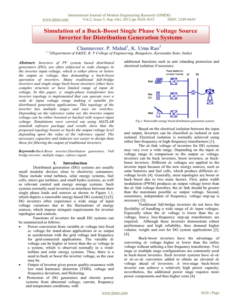
International Journal of Modern Engineering Research (IJMER) www.ijmer.com Vol.2, Issue.5, Sep.-Oct. 2012 pp-3628-3632 ISSN: 2249-6645 Simulation of a Buck-Boost Single Phase Voltage Source Inverter for Distribution Generation Systems Channaveer. P. Malad1, K. Uma Rao2 1, 2 (Department of E&EE, R. V College of Engineering, Bangalore, Karnataka State, India) Abstract: Inverters of PV system based distributed generators (DG), are often subjected to wide changes in the inverter input voltage, which is either above or below the output ac voltage, thus demanding a buck-boost operation of inverters. Many traditional full-bridge inverters and single-stage buck-boost inverters either have complex structure or have limited range of input dc voltage. In this paper, a` single-phase transformer less inverter topology is implemented that can operate over a wide dc input voltage range making it suitable for distributed generation applications. This topology of the inverter has multiple stages and uses six switches. Depending on the reference value set, the inverter output voltage can be either boosted or bucked with respect input voltage. Simulations were carried out using MATLAB simulink software package and results show that the proposed topology boosts or bucks the output voltage level depending upon the value of the reference signal. The necessary capacitor and inductor are easier to design than those for filtering the output of traditional inverters. Keywords-Buck-Boost inverter,Distribution generators, Full bridge inverter, multiple stages, refence signal. I. Introduction Distributed generation (DG) systems are usually small modular devices close to electricity consumers. These include wind turbines, solar energy systems, fuel cells, micro gas turbines, and small hydro systems, as well as relevant control and energy storage systems. Such systems normally need inverters as interfaces between their single phase loads and sources as shown in Figure 1.1, which depicts a renewable energy based DG system[1]-[5]. DG inverters often experience a wide range of input voltage variations due to the fluctuations of energy sources, which impose stringent requirements for inverter topologies and controls. Functions of inverters for small DG systems can be summarized as follows. Power conversion from variable dc voltage into fixed ac voltage for stand-alone applications or ac output in synchronism with the grid voltage and frequency for grid-connected applications. The variable dc voltage can be higher or lower than the ac voltage in a system, which is observed normally in a windturbine and solar energy systems. Thus, there is a need to buck or boost the inverter voltage, as the case may be. Output of inverter gives power quality assurance with low total harmonic distortion (THD), voltage and frequency deviation, and flickering. Protection of DG generators and electric power systems from abnormal voltage, current, frequency and temperature conditions, with additional functions such as anti islanding protection and electrical isolation if necessary. Fig 1: Renewable energy based distribution generation system. Based on the electrical isolation between the input and output, Inverters can be classified as isolated or non isolated. Electrical isolation is normally achieved using either line-frequency or high-frequency transformers [1]. The dc-link voltage of inverters for DG systems may vary over a wide range. Depending on the input dc voltage range in comparison to the output ac voltage, inverters can be buck inverters, boost inverters, or buckboost inverters. Different dc voltages are applied to the inverter input because of the new energy sources, such as solar batteries and fuel cells, which produce different dcvoltage levels [4]. Generally, most topologies are boost or buck–boost due to two main factors. First, pulse width modulation (PWM) produces an output voltage lower than the dc link voltage therefore, the dc link should be greater than the maximum possible ac output voltage. Second, sometimes, independent of frequency, voltage step-up is necessary [3]. Traditional full-bridge inverters do not have the flexibility of handling a wide range of dc input voltages. Especially when the dc voltage is lower than the ac voltage, heavy line-frequency step-up transformers are required. Although these inverters demonstrate robust performance and high reliability, they demand higher volume, weight and cost for DG system applications [2], [4]. Buck-boost inverters have the advantage of converting dc voltage higher or lower than the utility voltage without utilizing a line frequency transformer. Two stage or multiple stage configurations are commonly used in buck-boost inverters. Such inverter systems have dc-dc or dc-ac-dc converters added to obtain an elevated dc voltage ahead of inversion. A two-stage buck-boost inverter can achieve a relatively high power capacity; nevertheless, the additional power stage requires more power components and thus higher costs [4]. www.ijmer.com 3628 | Page International Journal of Modern Engineering Research (IJMER) www.ijmer.com Vol.2, Issue.5, Sep.-Oct. 2012 pp-3628-3632 ISSN: 2249-6645 II. Block Diagram of Buck-Boost Single Phase Voltage Source Inverter For Distribution Generation Fig 5: Equivalent circuit for unidirectional buck-boost operation of converter with H-bridge inverter. Fig .2: General Block diagram of buck-boost single phase voltage source inverter for distribution generation Block diagram of buck-boost inverter single phase voltage source inverter for distribution generation is shown in Fig.2. From block diagram it can be seen that voltage supplied from energy source (Photo voltaic, wind turbines, fuel cell) goes through two stages of conversion before it is supplied to grid. The voltage from the energy source (dc) is first converted into variable dc using a dc-dc converter. This variable dc voltage is then converted to ac voltage and is given to grid. The capacitor link acts as a voltage source to the inverter . III. When switch Z1 is ON, input voltage provides energy to inductor and the diode is reversed biased. When switch Z1 is turned OFF, the energy stored in the inductor is transferred to the capacitor C1. The regulated dc voltage across the Capacitor C1 acts as the dc link voltage to Hbridge inverter. By switching switches Z3, Z6 and Z4,Z5 of H-bridge complementally at power frequency ac voltage can be obtained. This voltage can be supplied to grid. 3.2 Flow chart and design consideration for the simulation. Proposed dc to ac converter The block diagram of multiple stage buck-boost inverter used for the proposed system is shown in Fig 3. Dc voltage obtained from the photo voltaic cells is given as input to dc- dc converter. Depending upon the reference value set, dc-dc converter either boosts or bucks the input voltage to 325Vdc. Dc voltage is converted to ac voltage by switching the switches of two arms of H-bridge complementarily. The obtained 230V, 50Hz, ac voltage is fed to grid. Fig 6: Flow chart to generate PWM for switches Z1 . Fig 3: Block diagram of buck-boost voltage source inverter. The dc link voltage is produced by buck–boost converter, prior to being converted to ac by the low frequency output H-bridge. A sine reference gives a sinusoidal voltage output that can be used in applications, such as drives, distributed generation, and power systems. Fig 4 gives the schematic of proposed inverter circuit. Fig 4: Proposed dc to ac converter schematic 3.1. Working principle. For unidirectional operation of the proposed topology of the inverter Z2 is kept turned OFF throughout the operation. It can be used for bidirectional operation. Switches Z1 and four switches of H-bridge Z3, Z4,Z5,Z6,turned ON and OFF. Average output voltage of buck-boost converter across the capacitor depends upon the duty cycle D. Equivalent circuit for unidirectional buck-boost operation of the converter is shown in Fig 5. Flow chart to generate PWM for the switch Z1 is shown in Fig 6. From flow chart it can seen that the nominal value of reference sine wave amplitude is 16V. If the reference sine wave amplitude is greater than 16V, the proposed inverter topology acts as a boost inverter whereas if it is less than 16V it acts as a buck inverter. However for if reference sine wave amplitude is equal to 16V, then the proposed topology of the inverter neither boosts the input voltage nor bucks the input voltage, it converts the dc input voltage to corresponding output ac voltage at 50Hz. Since the inductor current is discontinuous, the maximum Period for L1 to deliver energy from or to the dc source is limited to half the switching period. Thus, the maximum inductor current IL1 max, which is chosen according to switch and diode maximum current ratings, is given by (1) Therefore, the maximum allowable output current iomax (which is different to the maximum rated output current) must be less than. IL1 max |iomax| < |iL1 max| (2) When L1 is magnetized from the dc source with iL1 max in the first half of the switching period, L1 should deliver all its stored energy in the remainder of the period. www.ijmer.com 3629 | Page International Journal of Modern Engineering Research (IJMER) www.ijmer.com Vol.2, Issue.5, Sep.-Oct. 2012 pp-3628-3632 ISSN: 2249-6645 The longest time needed for L1 energy to be released is when C1 voltage and the output current are both zero. Assuming C1 voltage is zero and L1 initial current (the instant the inductor starts to charge the capacitor) is iL1 max, then (3) To allow iL1 to reach zero, the second period must be greater than or equal to a quarter of the reciprocal of the L1–C1 natural frequency, i.e. Fig 8: Simulation circuit for unidirectional buck-boost single phase (4) When the inductor transforms energy from the capacitor, back to the dc source, the peak inductor current at the end of the first period should not exceed iL1 max. The worst case occurs when the capacitor voltage is a maximum, then the inductor current is voltage source inverter. Table 1: System parameters L1 100µH Pv 0.3V/A Fsw 20kHz C1 50µF Kv 600V/A/s Fs 50Hz Pi 0.04 (5) Thus (6). IV. Simulations and practical results The block diagram used for the simulation is shown in the Fig 7. It uses PI and P controller to generate the PWM signal for Z1 and Z2 switches. The PWM for Hbridge can given through pulse generator since it is operated at 50Hz. Simulations have been carried out using MATLAB simulink software package. The proposed topology of the inverter has been implemented using circuit parameters given in Table 1. The input voltage is varied from 100 to 400V (dc) with corresponding change in the amplitude of the reference of sine wave. The circuit working is examined both in boost and buck mode. Simulation circuit for unidirectional buck-boost single phase voltage source inverter is shown in Fig 8. Fig 9 shows the simulink model of H-bridge with LC filter. Fig 9: Simulink model of H bridge inverter with LC filter The proposed topology of the inverter is implemented using circuit parameters given in table 1. The input voltage is varied from 100 to 400V (DC) with corresponding change in amplitude of the reference value of sine wave. The circuit working is examined both in boost and buck mode. Following are the analysis of the same. 4.1 Boost operation. Fig 10: The snap shot of output voltage 650V peak-peak, 50Hz, ac with input voltage of 100V DC and reference sine wave voltage amplitude set at 45V Fig 7: Block diagram of the buck-boost single phase voltage source inverter. In this case the proposed topology of the inverter circuit acts a boost inverter since the reference sine wave voltage amplitude applied is 45V. The reference sine wave voltage amplitude set in controller circuit is greater than 16V, the proposed topology the inverter acts as a boost inverter, converting 100V dc input voltage to output voltage of 650V peak–peak ac, 50Hz Fig 10 shows the boost operation of the proposed inverter topology. When input dc voltage is 100V and reference sine wave voltage amplitude set at 45V, the output voltage obtained is 650V peak-peak, 50Hz, ac. www.ijmer.com 3630 | Page International Journal of Modern Engineering Research (IJMER) www.ijmer.com Vol.2, Issue.5, Sep.-Oct. 2012 pp-3628-3632 ISSN: 2249-6645 Fig 11: The snap shot of output voltage 650V peak-peak, 50Hz, ac with input voltage of 200V DC and reference sine wave voltage amplitude set at 26V. Fig 13 shows operation of the proposed topology of the inverter circuit, as a buck inverter since the reference sine wave voltage amplitude applied is 13V. The reference sine wave voltage amplitude set in controller circuit is lesser than 16V, the proposed topology the inverter acts as a buck inverter, converting 400V dc input voltage to output voltage of 650V peak –peak, 50Hz, ac. Different output voltages for different input dc voltages that are carried during simulation are briefly summarized in Table 2. Fig 11 shows operation of the proposed topology of the inverter circuit, as a boost inverter since the reference sine wave voltage amplitude applied is 26V. The reference sine wave voltage amplitude set in controller circuit is greater than 16V, the proposed topology the inverter acts as a boost inverter, converting 200V dc input voltage to output voltage of 650V peak –peak, 50Hz ac. Sl.No Table 2: Summary of simulation results Vref Vdc Vpeak -peak 1 2 3 4 6 7 8 45V 32V 26V 18V 16V 15V 13V V. Fig 12: The snap shot of output voltage 650V, peak-peak, 50Hz,ac, when input voltage of 325V dc is applied and reference sine wave voltage amplitude set at 16V. Fig 12 shows operation of the proposed inverter circuit topology acting neither as a boost inverter nor a buck inverter since the reference sine wave voltage amplitude applied is 16V. The reference sine wave voltage amplitude given to controller circuit is equal to 16V, which is the nominal value of the voltage for the designed control circuit. For this value of the reference voltage, the proposed topology of the inverter converts input dc voltage to corresponding value of output ac voltage without boosting or bucking the magnitude input voltage. Thus converting input voltage of 325V dc to output voltage of 650V, peak-peak, and 50Hz ac. 4.2 Buck operation Whenever input voltage from PV cells to inverter circuit is greater than grid voltage then the inverter operates in buck mode. In order to operate the inverter in buck mode, amplitude of reference voltage should be set to value less than 16V. 100V 150V 200V 300V 325V 350V 400V 650V 650V 650V 650V 650V 650V 650V Conclusion Simulation of unidirectional of buck- boost single phase voltage source inverter has been carried out using MATLAB simulink software package. From simulation results it is seen the proposed topology of buck-boost single phase voltage inverter works exceptionally well producing an ac sine wave output depending upon the reference sine wave amplitude given to control circuit. The input voltage to power circuit was varied from 100V to 400V. From simulations results it can seen that if the reference sine wave amplitude is set 16V, which is the nominal value for the simulation control circuit, the voltage source buck-boost inverter neither bucks or boosts the input voltage however it inverters the dc voltage to 650V peak-peak 50Hz, ac voltage. If the reverence sine wave amplitude given to control circuit is greater than 16V then the proposed topology of inverter acts as boost inverter, inverting the input voltage to 650V peak-peak ac, 50Hz and vice versa. From simulation results it can summarized that the proposed topology of the inverter circuit operates for wide range of dc input voltage producing a sinusoidal ac voltage, 50Hz output. The proposed inverter is applicable as a utility interactive inverter for distributed generating systems and harmonic elimination applications. The proposed inverter uses six switches. The low switching frequency of the output H-bridge reduces inverter switching losses and costs, compared to six and eight switch-based techniques. The drawbacks of this inverter, compared to the traditional H-bridge inverter are: relatively high cost (six switches) and relatively high switching losses in two of the six switches. Reference [1] [2] Fig 13: The snap shot of output voltage 650V, peak-peak, 50Hz ac, when input voltage of 400V dc is applied and reference voltage amplitude set at 13V [3] www.ijmer.com T. G.Wilson, “The evolution of power electronics,” IEEE Trans. Power Electron., vol. 15, pp. 439–446, May 2000. X. Yaosuo, C. Liuchen, B. K. Kjaer, J. Bordonau, and T. Shimizu, “Topologies of single-phase inverters for small distributed power generators: An overview,” IEEE Trans. Power Electron., vol. 19, no. 5, pp. 1305–1314,Sep. 2004. R. Gonzalez, E. Gubia, J. Lopez, and L.Marroyo, “Transformerless single phase multilevel-based photovoltaic inverter,” IEEE Trans. Ind. Electron., vol. 55, no. 7, pp. 2694–2702, Jul. 2008. 3631 | Page International Journal of Modern Engineering Research (IJMER) www.ijmer.com Vol.2, Issue.5, Sep.-Oct. 2012 pp-3628-3632 ISSN: 2249-6645 Ahmed Mohamed Salamah, Stephen J. Finney “SinglePhase Voltage Source Inverter with a Bidirectional Buck– Boost Stage for Harmonic Injection and Distributed Generation” IEEE transactions on power electronics, vol. 24, no. 2, pp 376- 387, February 2009. [5] Roman, I.T. “A single-phase current-source inverter with active power filter for grid-tied PV systems”, 3rd IEEE International Symposium on Power Electronics for Distributed Generation Systems (PEDG), Aalborg, pp. 349-356, June 2012. [6] T. Boutot and L. Chang, “Development of a single-phase inverter for small wind turbines,” in Proc. IEEE Elect. Comput. Eng. Can. Conf. (CCECE 1998), Waterloo, ON, Canada, May 24–28, pp. 305–308. [7] P. Lezana, J. Rodrıguez, and D. A. Oyarzun, “Cascaded multilevel inverter with regeneration capability and reduced number of switches,” IEEE Trans. Ind. Electron., vol. 55, no. 3, pp. 697–703, Mar. 2008. [8] Yan Zhang “Comparison of traditional two-stage buckboost voltage source inverter and diode-assisted buck-boost voltage source inverter” Twenty-Seventh Annual IEEE trans on Applied Power Electronics Conference and Exposition (APEC), Orlando, FL, pp 141-148, Feb 2012. [9] Samuel, P. “Grid Interface of Wind Power With Large Split-Winding Alternator Using Cascaded Multilevel Inverter” IEEE Transactions on Energy Conversion, Volume: 26, Issue: 1, pp 299-309, March 2011. [10] Jalbrzykowski, S, Citko, T. “Current-Fed Resonant FullBridge Boost DC/AC/DC Converter” IEEE Transactions on Industrial Electronics, Volume: 55, Issue:3, pp 1198 – 1205, March 2008. [4] www.ijmer.com 3632 | Page


