A Soft Switching Scheme for DC-DC Converter by
advertisement

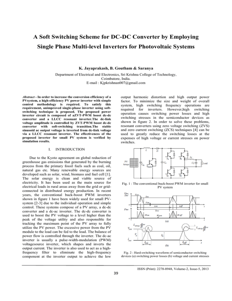
A Soft Switching Scheme for DC-DC Converter by Employing Single Phase Multi-level Inverters for Photovoltaic Systems K. Jayaprakash, B. Goutham & Saranya Department of Electrical and Electronics, Sri Krishna College of Technology, Coimbatore, India. E-mail : Kjpkrishnan007@gmail.com output harmonic distortion and high output power factor. To minimize the size and weight of overall system, high switching frequency operations are required for inverters. However,high switching operation causes switching power losses and high switching stresses in the semiconductor devices as shown in figure 2. In order to solve these problems, resonant converters using zero voltage switching (ZVS) and zero current switching (ZCS) techniques [4] can be used to greatly reduce the switching losses at the expenses of high voltage or current stresses on power switches. Abstract - In order to increase the conversion efficiency of a PVsystem, a high-efficiency PV power inverter with simple control methodology is required. To satisfy this requirement, animproved single-phase inverter using softswitching technique is proposed. The proposed power inverter circuit is composed of aZVT-PWM boost dc-dc converter and a LLCC resonant inverter.The dc-link voltage amplitude is controlled by ZVT-PWM boost dc-dc converter with soft-switching transition.The stable sinusoid ac output voltage is inverted from dc-link voltage via a LLCC resonant inverter. The effectiveness of the proposed inverter for small PV system is verified by simulation results. I. INTRODUCTION Due to the Kyoto agreement on global reduction of greenhouse gas emissions that generated by the burning process from the primary fossil fuels such as coal, oil, natural gas etc. Many renewable energy sources are developed such as solar, wind, biomass and fuel cell [1]. The solar energy is clean and viable source of electricity. It has been used as the main source for electrical loads in rural areas away from the grid or gridconnected in distributed energy production. In recent years, the conventional buck-boost PWM inverters shown in figure 1 have been widely used for small PVsystem [2-3] due to the individual operation and simple control. These systems compose of a PV array, a dc-dc converter and a dc-ac inverter. The dc-dc converter is used to boost the PV voltage to a level higher than the peak of the voltage utility and also responsible for tracking the maximum point of the PV array to fully utilize the PV power. The excessive power from the PV module to the load can be fed to the load. The balance of power flow is controlled through the inverter. The dc-ac inverter is usually a pulse-width-modulation (PWM) voltagesource inverter, which shapes and inverts the output current. The inverter is also used to act as a highfrequency filter to eliminate the high-frequency component at the inverter output to achieve the low Fig. 1 : The conventional buck-boost PWM inverter for small PV system Fig. 2 : Hard-switching waveform of semiconductor switching devices (a) switching power losses (b) voltage and current stresses ISSN (Print): 2278-8948, Volume-2, Issue-5, 2013 39 International Journal of Advanced Electrical and Electronics Engineering, (IJAEEE) For the inverter without reactive energy feedback paths, the parasitic reactive energy due to the possible leakage of inductors also imposes transient high voltage, dv/dt or di/dtstresses on switch devices that causes high electro magnetic interference (EMI). Therefore, soft-transition switching techniques such as zero voltage transition (ZVT) [5] and zero current transition (ZCT) [6] have been developed to minimize or eliminate both switching losses and stresses, and thus improving converter efficiency. In this paper, a soft-switching single-phase inverter for small PV system is proposed. This inverter is composed of a ZVT-PWM boost dc-dc converter and a LLCC resonant inverter [7]. An auxiliary circuit isused to provide the active switches in a boos converter operate at soft-switching without additional voltage and current stresses. The stable ac output voltage is generated from the LLCC resonant inverter with low total harmonic distortion (THD). In the following, the operating principles of the proposed PV-system will be thoroughly discussed. Simulation results will be given to validate the effectiveness of the fulfilled functions. The proposed single-phase inverter for small PV-system is shown in figure 3. The inverter circuit is composed of a ZVTPWM boost dc-dc converter that uses PWM control and a dc-ac LLCC resonant inverter. According to the PV array characteristic, the output voltage of PV array varies with light intensity. The boost dc-dc converter with dc voltage feedback control is utilized to provide the constant dc voltage Vdc for the inverter. The dc-link voltage amplitude is controlled by the boost dc-dc converter. B. LLCC-Resonant Inverter The LLCC-resonant inverter has full-bridge switches (Sinv1, Sinv2, Sinv3 and Sinv4) that transfer the dc-link voltage to a square wave with amplitude Vdc The inverter is operated at a geometric mean frequency to provide stable sinusoid ac voltage (vO) output. The input voltage of the resonant circuit isa square wave of the following form. The fundamental component of the square wave is A. ZVT-PWM Boost DC-DC Converter Fig. 4. shows the key waveforms of the ZVT-PWM boost dc-dc converter. By adding the resonant network with a conventional PWM boost dc-dc converter, the converter achieves zero-voltage switching for both the active and passive switches without increasing the voltage and current stresses. The additional resonant network is composed of a resonant inductor (Lr), resonant capacitor (Cr), an auxiliary switch (SZVT)and diode (D1). in which fSis the switching frequency, and The output voltage of the resonant tank is Where VO and _ represent the amplitude and phase of theoutput voltage vO. The input impedance of the LLCC-resonant tank can be represented as Where the admittance of the parallel-resonant tank is Fig. 3 : Schematic diagram for proposed configuration ISSN (Print): 2278-8948, Volume-2, Issue-5, 2013 40 International Journal of Advanced Electrical and Electronics Engineering, (IJAEEE) When the switching frequency is operated at the geometricmean frequency, the real and imaginary part of the voltage gain are equal to one and zero, respectively. Therefore, the amplitude of the voltage gain is not influenced by the variation of the quality factor, and the amplitude of the output voltage, Vois equal to 4Vdc/π. The amplitude and phase of GLLCC as the function of fSat different values of Q are shown in figure 5. III. SIMULATION RESULTS To evaluate the performance of the proposed system, the prototype circuit is designed and simulated with OrcadPSpiceas shown in figure 6. A 40kHz ZVTPWM boost converter is utilized to provide constant dc voltage Vdc = 245Vdc for the LLCC resonant inverter. Fig. 4 : Waveform of the ZVT –PWM boost dc-dc converter The voltage gain of the LLCC-resonant tank GLLCC is defined as the ratio of the ac output voltage and the fundamental of square input voltage When the resonant condition occurs, the real part of the denominator of is equal to zero, that is The two resonant frequencies in radian (ω01, ω02) of the LLC Cresonant circuit can be obtained as Where K=(1/(LSCP))(1+(CP/CS)+(LS/LP)). Define the ratio LP/LS= CS/CP, then the geometric mean frequency in radian can be obtained as Fig. 5 A 120W output LLCC resonant inverter is operated at 50Hz switching frequency. The geometric mean frequency is obtained at 50 Hz. The parameters of the LLCC resonant tank are given as ISSN (Print): 2278-8948, Volume-2, Issue-5, 2013 41 International Journal of Advanced Electrical and Electronics Engineering, (IJAEEE) IV. CONCLUSION An improved single-phase inverter for small PVsystem using resonant-technique has been proposed to overcome the drawbacks of the conventional singlephase PV power inverter. This inverter composes of a ZVT-PWM boost dc-dc converter and a LLCC-resonant inverter. The active switches in a ZVT-PWM boost dcdc converter operate in soft-switching condition and without voltage and current stresses. This reduces switching losses, thereby increasing the efficiency of the converter. The LLCC resonant inverter incorporates series and parallel combinations of inductors and capacitors otherwise know as a series-resonant tank and parallel-resonant tank to provide a stable ac output voltage with low THD. The simulation results show that the ZVT-PWM boost dc-dc converter and the LLCCresonant inverter can be applied to the small scale PV system with high performance. The main switch current iS and the voltage across the main switch vCr of the boost converter are shown in figure 7. The waveforms confirm the zero-voltageswitching of the main switch of the boost converter. The simulation input and output voltage waveform results from the LLCC resonant inverter are depicted in figure 8. It can be observed that the input and output voltages of the LLCC resonant tank are in phase when the switching frequency of the inverter is operated at the geometric mean frequency .The THD of output voltage is also shown in figure 8. VI. REFERENCES [1] B. K. Bose, “Energy, environment, and advances in power electronics,” IEEE Trans. on Power Electronics, vol. 15, pp. 688-701, July 2000. [2] J. A. Gow and C. D. Manning, “Photovoltaic converter system suitable for use in small scale stand-alone or grid connected applications,” IEE Proceedings on Electric Power Applications, vol. 147, pp. 535-543, June 2000. [3] K. Matsui, I. Yamamoto, K. Ando, and T. Kobayashi, “Utility-interactive photovoltaic power conditioning systems with forward converter for domestic applications,” IEE Proceedings on Electric Power Applications, vol. 147, pp. 199-205, March 2000. [4] G. Hua and F. C. Lee, “Soft-switching techniques in PWM converter,” IEEE Trans. on Industrial Electronics, vol. 42, pp. 595-603, December 1995. [5] G. Hua, C. S. Leu and F. C. Lee, “Novel zerovoltage-transition PWM converters,” IEEE proc. of PESC, pp. 55-60, 1992. Fig. 7 : Voltage and current of the boost converter switch Fig. 8: Output voltage spectrum of the LLCC resonant inverter ISSN (Print): 2278-8948, Volume-2, Issue-5, 2013 42


