VS4407AS Absolute Maximum Ratings V Features Description
advertisement
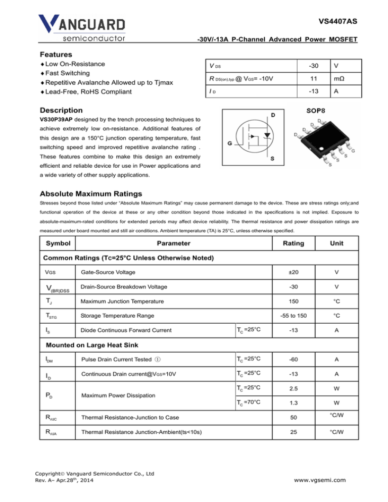
VS4407AS -30V/-13A P-Channel Advanced Power MOSFET Features Low On-Resistance Fast Switching Repetitive Avalanche Allowed up to Tjmax Lead-Free, RoHS Compliant V DS -30 V R DS(on),typ @ VGS= -10V 11 mΩ ID -13 A Description VS30P39AP designed by the trench processing techniques to achieve extremely low on-resistance. Additional features of this design are a 150°C junction operating temperature, fast switching speed and improved repetitive avalanche rating . These features combine to make this design an extremely efficient and reliable device for use in Power applications and a wide variety of other supply applications. Absolute Maximum Ratings Stresses beyond those listed under “Absolute Maximum Ratings” may cause permanent damage to the device. These are stress ratings only;and functional operation of the device at these or any other condition beyond those indicated in the specifications is not implied. Exposure to absolute-maximum-rated conditions for extended periods may affect device reliability. The thermal resistance and power dissipation ratings are measured under board mounted and still air conditions. Ambient temperature (TA) is 25°C, unless otherwise specified. Symbol Parameter Rating Unit Common Ratings (TC=25°C Unless Otherwise Noted) VGS Gate-Source Voltage ±20 V V(BR)DSS Drain-Source Breakdown Voltage -30 V TJ Maximum Junction Temperature 150 °C TSTG Storage Temperature Range -55 to 150 °C IS Diode Continuous Forward Current TC =25°C -13 A Mounted on Large Heat Sink IDM Pulse Drain Current Tested ① TC =25°C -60 A ID Continuous Drain current@VGS=10V TC =25°C -13 A PD TC =25°C 2.5 W Maximum Power Dissipation TC =70°C 1.3 W R JC Thermal Resistance-Junction to Case 50 °C/W R JA Thermal Resistance Junction-Ambient(ts<10s) 25 °C/W Copyright Vanguard Semiconductor Co., Ltd Rev. A– Apr.28th, 2014 www.vgsemi.com VS4407AS -30V/-13A P-Channel Advanced Power MOSFET Symbol Parameter Condition Min. Typ. Max. Unit Static Electrical Characteristics @ TJ = 25°C (unless otherwise stated) Drain-Source Breakdown Voltage VGS=0V ID=-250μA -30 -- -- V Zero Gate Voltage Drain Current(Tc=25℃) VDS=-24V,VGS=0V -- -- -1 μA Zero Gate Voltage Drain Current(Tc=125℃) VDS=-24V,VGS=0V -- -- -100 μA IGSS Gate-Body Leakage Current VGS=±20V,VDS=0V -- -- ±100 nA VGS(TH) Gate Threshold Voltage VDS=VGS,ID=-250μA -1.0 -1.6 -2.5 V RDS(ON) Drain-Source On-State Resistance③ VGS=-10V, ID=-8A -- 11 16 mΩ RDS(ON) Drain-Source On-State Resistance③ VGS=-5V, ID=-8A -- 16 26 mΩ -- 1950 -- pF -- 320 -- pF -- 225 -- pF -- 28 -- nC -- 4.5 -- nC -- 9 -- nC -- 9 -- nS V(BR)DSS IDSS Dynamic Electrical Characteristics @ TJ = 25°C (unless otherwise stated) Ciss Input Capacitance Coss Output Capacitance Crss Reverse Transfer Capacitance Qg Total Gate Charge Qgs Gate-Source Charge Qgd Gate-Drain Charge VDS=-10V,VGS=0V, f=1MHz VDS=-10V,ID=-10A, VGS=-10V Switching Characteristics t d(on) Turn-on Delay Time tr Turn-on Rise Time ID=-1A, -- 10 -- nS t d(off) Turn-Off Delay Time RG=6.8Ω, -- 22 -- nS tf Turn-Off Fall Time -- 11 -- nS VDD=-15V, VGS=-10V Source- Drain Diode Characteristics@ TJ = 25°C (unless otherwise stated) ISD Source-drain current(Body Diode) Tc=25℃ -- -- -60 A VSD Forward on voltage ISD=-10A,VGS=0V -- -- -1.3 V t rr Reverse Recovery Time Tj=25℃,Isd=-8A, -- 26 -- nS Qrr Reverse Recovery Charge -- 35 -- nC VGS=0V di/dt=-100A/μs NOTE: ① Repetitive rating; pulse width limited by max. junction temperature. ② Limited by TJmax, starting TJ = 25°C, L = 0.5mH,RG = 25Ω, IAS =-12A, VGS =-10V. Part not recommended for use above this value ③ Pulse width ≤ 300μs; duty cycle≤ 2%. Copyright Vanguard Semiconductor Co., Ltd Rev. A– Apr.28th, 2014 www.vgsemi.com VS4407AS -30V/-13A P-Channel Advanced Power MOSFET -ID, -Drain-Source Current (A) -ID, -Drain-Source Current (A) Typical Characteristics -VDS,- Drain -Source Voltage (V) Fig2. Maximum Drain Current Vs.Case Temperature Normalized On Resistance -ID, -Drain-Source Current (A) Fig1. Typical Output Characteristics Tc - Case Temperature (°C) -ID,- Drain Current (A) Tj - Junction Temperature (°C) Fig4. Normalized On-Resistance Vs. Temperature P(pk), Peak Transitent Power(W) -VGS, -Gate -Source Voltage (V) Fig3. Typical Transfer Characteristics t1, Time (sec) Fig5.Typical Peak Transitent Power Copyright Vanguard Semiconductor Co., Ltd Rev. A– Apr.28th, 2014 -VDS, -Drain -Source Voltage (V) Fig6. Maximum Safe Operating Area www.vgsemi.com VS4407AS -VGS, -Gate-Source Voltage (V) -ISD, -Reverse Drain Current (A) -30V/-13A P-Channel Advanced Power MOSFET -VSD, -Source-Drain Voltage (V) Qg -Total Gate Charge (nC) Fig8. Typical Gate Charge Vs.Gate-Source Voltage C, Capacitance (pF) VGS(TH), Gate -Source Voltage (V) Fig7. Typical Source-Drain Diode Forward Voltage Tj - Junction Temperature (°C) -VDS , -Drain-Source Voltage (V) Fig9. Threshold Voltage Vs. Temperature Fig11. Unclamped Inductive Test Circuit and Copyright Vanguard Semiconductor Co., Ltd Rev. A– Apr.28th, 2014 Fig10. Typical Capacitance Vs.Drain-Source Voltage Waveforms Fig12. Switching Time Test Circuit and waveforms www.vgsemi.com VS4407AS -30V/-13A P-Channel Advanced Power MOSFET SOP8 Package Outline DIMENSIONS ( unit : mm ) Symbol Min Typ Max Symbol Min Typ Max A -- 1.75 -- A1 0.10 0.18 0.25 A2 1.25 1.35 1.45 A3 -- 0.25 -- bp 0.36 0.42 0.49 c 0.19 0.22 0.25 D 4.80 4.92 5.00 E 3.80 3.90 4.00 e -- 1.27 -- HE 5.80 5.98 6.20 L -- 1.05 -- Lp 0.40 0.68 1.00 Q 0.60 0.65 0.70 v -- 0.25 -- w -- 0.25 -- y -- 0.10 -- Z 0.30 0.50 0.70 θ 0° 8° Product Marking Package Packaging Min Unit Quantity VS4407AS VS4407AS SOP8 3000/Reel 6000 Customer Service Sales and Service: sales@vgsemi.com Vanguard Semiconductor CO., LTD TEL: (86-755) -26902410 FAX: (86-755) -26907027 WEB: www.vgsemi.com Copyright Vanguard Semiconductor Co., Ltd Rev. A– Apr.28th, 2014 www.vgsemi.com
