LET16060C
RF power transistor from the LdmoST family
of N-channel enhancement-mode lateral MOSFETs
Datasheet - production data
Features
• Excellent thermal stability
• Common source configuration
• POUT (@ 28 V)= 60 W with 13.8 dB gain @
1600 MHz
• BeO free package
• In compliance with the 2002/95/EC European
directive
M243
epoxy sealed
Description
The LET16060C is a common source N-channel
enhancement-mode lateral field-effect RF power
transistor designed for broadband commercial
and industrial applications at frequencies up to
1.6 GHz. The LET16060C is designed for high
gain and broadband performance operating in
common source mode at 28 V. It is ideal for
INMARSAT satellite communications.
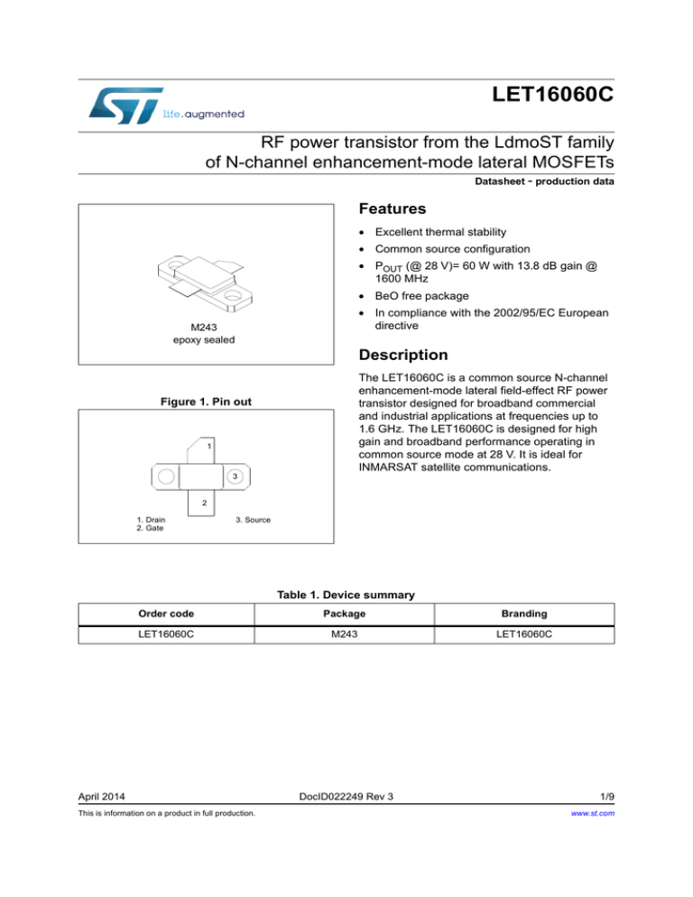
Figure 1. Pin out
1
3
2
1. Drain
2. Gate
3. Source
Table 1. Device summary
Order code
Package
Branding
LET16060C
M243
LET16060C
April 2014
This is information on a product in full production.
DocID022249 Rev 3
1/9
www.st.com
Maximum ratings
1
LET16060C
Maximum ratings
Table 2. Absolute maximum ratings (TCASE = 25 °C)
Symbol
Parameter
Value
Unit
V(BR)DSS
Drain-source voltage
80
V
VGS
Gate-source voltage
-0.5 to +15
V
Drain current
12
A
Power dissipation (@ TC = 70 °C)
100
W
Max. operating junction temperature
200
°C
-65 to +150
°C
Value
Unit
1.3
°C/W
ID
PDISS
TJ
TSTG
Storage temperature
Table 3. Thermal data
Symbol
Rth(JC)
2/9
Parameter
Junction-case thermal resistance
DocID022249 Rev 3
LET16060C
2
Electrical characteristics
Electrical characteristics
TC = 25 °C
Table 4. Static
Symbol
Test conditions
V(BR)DSS VGS = 0 V; IDS = 10 mA
Min.
Typ.
Max.
Unit
80
V
IDSS
VGS = 0 V; VDS = 28 V
1
μA
IGSS
VGS = 5 V; VDS = 0 V
1
μA
5
V
1.2
V
VGS(Q)
VDS = 28 V; ID = 400 mA
VDS(ON)
VGS = 10 V; ID = 3 A
GFS
VDS = 10 V; ID = 3 A
CISS
VGS = 0 V; VDS = 28 V; f = 1 MHz
77
pF
COSS
VGS = 0 V; VDS = 28 V; f = 1 MHz
39
pF
CRSS
VGS = 0 V; VDS = 28 V; f = 1 MHz
1.2
pF
2
0.8
2.5
mho
Table 5. Dynamic
Symbol
Test conditions
POUT
VDD = 28 V; IDQ = 400 mA; PIN = 4 W; f = 1600 MHz
GPS
VDD = 28 V; IDQ = 400 mA; POUT = 60 W; f = 1600 MHz
VDD = 28 V; IDQ = 400 mA; PIN = 4 W; f = 1600 MHz
hD
Load
VDD = 28 V; IDQ = 400 mA; POUT = 60 W; f = 1600 MHz
mismatch All phase angles
Min.
Typ.
Max.
60
70
W
12.5
13.8
dB
50
55
-
20:1
Unit
%
VSWR
Table 6. Thermal data
Symbol
Rthj-case
Parameter
Thermal resistance junction-case max
Value
Unit
1.3
°C/W
Table 7. Impedance data
Frequency (MHz)
Z source (Ω)
Z load (Ω)
1600
1.3 - j2.3
0.2 - j.96
DocID022249 Rev 3
3/9
9
Typical performances
3
LET16060C
Typical performances
Figure 2. Gain and efficiency vs output power Figure 3. Gain vs ouptut power and bias current
*DLQG%
)UHT 0+]
9'' 9
,'4 P$
*DLQG%
(IILFLHQF\
(IILFLHQF\
*DLQ
,GT P$
)UHT 0+]
9'' 9
$09
2XWSXWSRZHU:
Figure 4. Ouptut power vs drain supply voltage
)UHT 0+]
,'4 P$
3LQ :
3LQ :
3LQ :
6XSSO\YROWDJH9
$09
4/9
2XWSXWSRZHU:
2XWSXWSRZHU:
,GT P$
,GT P$
DocID022249 Rev 3
$09
LET16060C
Board layout, schematic and BOM
Figure 5. Board layout
C10
C11
+
C13
+
B1
+
4
Board layout, schematic and BOM
R1
R3
B2
R2
C9
C8
C4
L1
C
+
B3
C12
L2
C2
C1
+
B4
C6
C3
C7
C5
STMicroelectronics, Inc.
LET16045
LOG xxxx
REV
INPUT
STMicroelectronics, Inc.
LET16045
LOG xxxx
REV
OUTPUT
C
GIPG290420140950FSR
Figure 6. Schematic
R1
FB1
VGG
FB2
C13
FB3
R3
FB4
Vdd
R2
C10
C11
C12
C9
C8
L2
L1
TL7
TL1
TL2
TL3
TL4
C2
C1
TL5
TL8
TL9
TL10
TL12
TL11
C7
TL6
DUT
C4
C5
C6
C3
GIPG290420140944FSR
DocID022249 Rev 3
5/9
9
Board layout, schematic and BOM
LET16060C
Table 8. Component list
6/9
Item
Qty
Part number
Vendor
Description
R1
1
CR1206-8W-561JB
VENKEL
560 OHM, 1/8W surface mount chip
resistor
R2
1
CR1206-8W-132JB
VENKEL
1.3K OHM, 1/8W surface mount chip
resistor
R3
1
CR1206-8W-100JB
VENKEL
10 OHM, 1/8W surface mount chip
resistor
FB1,2,3,4,
4
2743021447
FAIR-RITE
CORP
Surface Mount EMI sheild bead
C1,C4,C5,C6
4
JOHANSON
0.6-4.5pF giga trim variable capacitor
C2,C7,C9,C12
4
ATC100B470XXXX
ATC
47 pF chip capacitor
C3
1
27291PC
JOHANSON
0.8-8pF giga trim variable capacitor
C8
1
ATC100B330XXXX
ATC
33pF chip capacitor
C10
1
330uF, 50V electrolytic capacitor
C11
1
10uF, 63V electrolytic capacitor
C13
1
100uF, 63V electrolytic capacitor
L1, L2
2
TL1, TL2
2
L= 1.350in [34.29mm]
W=0.082in [2.080mm]
TL3
1
L= 0.469in [11.91mm]
W=0.080in [2.020mm]
TL4, TL5
2
L= 0.277in [7.03mm]
W=0.323in [8.210mm]
TL6
1
L= 0.207in [5.26mm]
W=0.506in [12.85mm]
TL7
1
L= 0.208in [5.28mm]
W=0.506in [12.85mm]
TL8,TL9
2
L= 0.275in [6.98mm]
W=0.324in [8.230mm]
TL10,TL11
2
L= 0.470in [11.93mm]
W=0.080in [2.020mm]
TL12
1
L= 1.351in [34.33mm]
W=0.082in [2.080mm]
Board 3X5
1
1812SMS-33NJ
Coilcraft
Rogers Corp
DocID022249 Rev 3
33 nH coil
Er=2.55
t=0.0026in
h=0.030in
LET16060C
5
Package mechanical data
Package mechanical data
In order to meet environmental requirements, ST offers these devices in different grades of
ECOPACK® packages, depending on their level of environmental compliance. ECOPACK®
specifications, grade definitions and product status are available at: www.st.com.
ECOPACK® is an ST trademark.
Figure 7. M243 package dimensions
Table 9. M243 (.230 x .360 2L N/HERM W/FLG) mechanical data
mm
inch
Dim.
Min.
Typ
Max.
Min.
Typ
Max.
A
5.21
5.72
0.205
0.225
B
5.46
6.48
0.215
0.255
C
5.59
6.1
0.22
0.24
D
14.27
0.562
E
20.07
20.57
0.79
0.81
F
8.89
9.4
0.35
0.37
G
0.1
0.15
0.004
0.006
H
3.18
4.45
0.125
0.175
I
1.83
2.24
0.072
0.088
J
1.27
1.78
0.05
0.07
DocID022249 Rev 3
7/9
9
Revision history
6
LET16060C
Revision history
Table 10. Document revision history
8/9
Date
Revision
Changes
20-Sep-2011
1
Initial release.
15-Nov-2011
2
Modified Table 4: VGS(Q) and VDS(ON)
Modified Table 5 and 6
Inserted: Table 7
Inserted: Figure 2, 3 and 4
19-Apr-2014
3
Added Section 4: Board layout, schematic and BOM.
DocID022249 Rev 3
LET16060C
Please Read Carefully:
Information in this document is provided solely in connection with ST products. STMicroelectronics NV and its subsidiaries (“ST”) reserve the
right to make changes, corrections, modifications or improvements, to this document, and the products and services described herein at any
time, without notice.
All ST products are sold pursuant to ST’s terms and conditions of sale.
Purchasers are solely responsible for the choice, selection and use of the ST products and services described herein, and ST assumes no
liability whatsoever relating to the choice, selection or use of the ST products and services described herein.
No license, express or implied, by estoppel or otherwise, to any intellectual property rights is granted under this document. If any part of this
document refers to any third party products or services it shall not be deemed a license grant by ST for the use of such third party products
or services, or any intellectual property contained therein or considered as a warranty covering the use in any manner whatsoever of such
third party products or services or any intellectual property contained therein.
UNLESS OTHERWISE SET FORTH IN ST’S TERMS AND CONDITIONS OF SALE ST DISCLAIMS ANY EXPRESS OR IMPLIED
WARRANTY WITH RESPECT TO THE USE AND/OR SALE OF ST PRODUCTS INCLUDING WITHOUT LIMITATION IMPLIED
WARRANTIES OF MERCHANTABILITY, FITNESS FOR A PARTICULAR PURPOSE (AND THEIR EQUIVALENTS UNDER THE LAWS
OF ANY JURISDICTION), OR INFRINGEMENT OF ANY PATENT, COPYRIGHT OR OTHER INTELLECTUAL PROPERTY RIGHT.
ST PRODUCTS ARE NOT DESIGNED OR AUTHORIZED FOR USE IN: (A) SAFETY CRITICAL APPLICATIONS SUCH AS LIFE
SUPPORTING, ACTIVE IMPLANTED DEVICES OR SYSTEMS WITH PRODUCT FUNCTIONAL SAFETY REQUIREMENTS; (B)
AERONAUTIC APPLICATIONS; (C) AUTOMOTIVE APPLICATIONS OR ENVIRONMENTS, AND/OR (D) AEROSPACE APPLICATIONS
OR ENVIRONMENTS. WHERE ST PRODUCTS ARE NOT DESIGNED FOR SUCH USE, THE PURCHASER SHALL USE PRODUCTS AT
PURCHASER’S SOLE RISK, EVEN IF ST HAS BEEN INFORMED IN WRITING OF SUCH USAGE, UNLESS A PRODUCT IS
EXPRESSLY DESIGNATED BY ST AS BEING INTENDED FOR “AUTOMOTIVE, AUTOMOTIVE SAFETY OR MEDICAL” INDUSTRY
DOMAINS ACCORDING TO ST PRODUCT DESIGN SPECIFICATIONS. PRODUCTS FORMALLY ESCC, QML OR JAN QUALIFIED ARE
DEEMED SUITABLE FOR USE IN AEROSPACE BY THE CORRESPONDING GOVERNMENTAL AGENCY.
Resale of ST products with provisions different from the statements and/or technical features set forth in this document shall immediately void
any warranty granted by ST for the ST product or service described herein and shall not create or extend in any manner whatsoever, any
liability of ST.
ST and the ST logo are trademarks or registered trademarks of ST in various countries.
Information in this document supersedes and replaces all information previously supplied.
The ST logo is a registered trademark of STMicroelectronics. All other names are the property of their respective owners.
© 2014 STMicroelectronics - All rights reserved
STMicroelectronics group of companies
Australia - Belgium - Brazil - Canada - China - Czech Republic - Finland - France - Germany - Hong Kong - India - Israel - Italy - Japan Malaysia - Malta - Morocco - Philippines - Singapore - Spain - Sweden - Switzerland - United Kingdom - United States of America
www.st.com
DocID022249 Rev 3
9/9
9


