MP20075
3A, 1.05V–3.6V
DDR2/3/3L/4 Memory Termination Regulator
The Future of Analog IC Technology
DESCRIPTION
FEATURES
The
MP20075
precision
DDR2/3/3L/4
termination LDO regulator features a precision
VREF/2
tracking
voltage
for
accurate
termination. The VTT-LDO output can
sink/source up to 3A.
•
•
The MP20075 maintains a fast transient
response only requires 20μF (2x10μF) ceramic
output capacitance. The MP20075 supports
Kelvin sensing.
The MP20075 is available in the 8-pin MSOP
with Exposed PAD and is specified from −40oC
to 85oC.
•
•
•
•
•
•
•
•
•
VDDQ Voltage Range: 1.05V to 3.6 V
Up to 3A Integrated Sink/Source Linear
Regulator with Accurate VREF/2 Divider
Reference for DDR2/3/3L/4 Termination
Requires Only 20μF Ceramic Output
Capacitance
Drive Voltage: 3.3V
1.05V Input (VDDQ) Helps Reduce Total
Power Dissipation
Integrated Divider Tracks VREF for
accurate VTT and VTTREF Output Voltage
Kelvin Sensing (VTTSEN)
±30mV Accuracy for VTT
±18mV Accuracy for VTTREF
Built-In Soft-Start, UVLO and OCL
Thermal Shutdown
APPLICATIONS
•
•
Notebook DDR2/3/3L/4 Memory Supply
and Termination Voltage in ACPI Compliant
Systems
Active Termination Bus
All MPS parts are lead-free and adhere to the RoHS directive. For MPS green
status, please visit MPS website under Products, Quality Assurance page.
“MPS” and “The Future of Analog IC Technology” are registered trademarks of
Monolithic Power Systems, Inc.
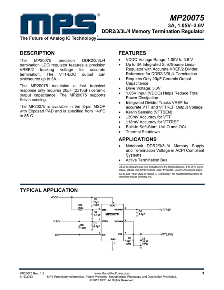
TYPICAL APPLICATION
MP20075 Rev. 1.2
7/15/2013
www.MonolithicPower.com
MPS Proprietary Information. Patent Protected. Unauthorized Photocopy and Duplication Prohibited.
© 2013 MPS. All Rights Reserved.
1
MP20075 – 3A, 1.05V-3.6V INPUT, DDR2/3/3L MEMORY TERMINATION REGUALTOR
ORDERING INFORMATION
Part Number*
MP20075DH
Package
MSOP8E
Top Marking
Free Air Temperature (TA)
20075
-40°C to +85°C
* For Tape & Reel, add suffix –Z (e.g. MP20075DH–Z);
For RoHS Compliant Packaging, add suffix –LF (e.g. MP20075DH–LF–Z)
PACKAGE REFERENCE
TOP VIEW
DDQ
1
8
VTTREF
VTT
2
7
EN
GND
3
6
REF
VTTSEN
4
5
VDRV
EXPOSED PAD
ON BACKSIDE
ABSOLUTE MAXIMUM RATINGS (1)
Supply Voltage VDDQ........................ -0.3V to 3.6V
Drive Voltage VDRV..................... -0.3V to 6.0V
All Other Pins................................ -0.3V to 6.0V
(2)
Continuous Power Dissipation (TA = +25°C)
........................................................... 1.56W
Junction Temperature...............................150oC
Lead Temperature ....................................260oC
Storage Temperature .............. -50oC to +150oC
Recommended Operating Conditions
(3)
Drive Voltage VDRV.................... 3.0V to 3.5V
Operating Junct. Temp (TJ) .......-40oC to +125oC
MP20075 Rev. 1.2
7/15/2013
Thermal Resistance
(4)
θJA
θJC
MSOP8E.................................. 50...... 12... oC/W
Notes:
1) Exceeding these ratings may damage the device.
2) The maximum allowable power dissipation is a function of the
maximum junction temperature TJ(MAX), the junction-toambient thermal resistance θJA, and the ambient temperature
TA. The maximum allowable continuous power dissipation at
any ambient temperature is calculated by PD(MAX)=(TJ(MAX)TA)/ θJA. Exceeding the maximum allowable power dissipation
will cause excessive die temperature, and the regulator will go
into thermal shutdown. Internal thermal shutdown circuitry
protects the device from permanent damage.
3) The device is not guaranteed to function outside of its operating
conditions.
4) Measured on JESD51-7 4-layer board.
www.MonolithicPower.com
MPS Proprietary Information. Patent Protected. Unauthorized Photocopy and Duplication Prohibited.
© 2013 MPS. All Rights Reserved.
2
MP20075 – 3A, 1.05V-3.6V INPUT, DDR2/3/3L MEMORY TERMINATION REGUALTOR
ELECTRICAL CHARACTERISTICS
VDRV = 3.3V, TA = +25oC, unless otherwise noted.
Parameters
Symbol
VDRV Operating Voltage
VDRV
VDRV Shut down current
IDRV_SD
VDRV Operation Current
IDRV
Thermal Trip Point
TSD
Hysteresis
TSDHYS
VDDQ
UVLO
Upper
VDDQUV+
Threshold
VTT with Respect to 1/2VREF
dVTT0
Test Condition
Min
Typ
Max
Unit
ITT=3A
VDRV =3.3 V, VDDQ=0V
VEN_H, VTT=0.75V
3.0
3.3
0.2
1.3
150
25
3.5
1.0
3
V
μA
mA
o
C
o
C
0.9
1.0
V
-30
-30
30
30
mV
-30
-30
30
30
mV
-30
-30
30
30
mV
Rising Edge; hysteresis = 55mV
1/2VREF – VTT, VREF = 1.8V,
IVTT = 0 to 3A (Sink Current)
IVTT = 0 to 3A (Source Current)
1/2VREF – VTT, VREF = 1.5V,
IVTT = 0 to 3A (Sink Current)
IVTT = 0 to 3A (Source Current)
1/2VREF -VTT, VREF=1.35V
IVTT = 0 to 3A (Sink Current)
IVTT = 0 to 3A (Source Current)
Source Current Limit
ILIMVTsrc
4.0
A
Sink Current Limit
ILIMVTsnk
4.0
A
ILIMVTSS
1.0
A
Soft−Start
Limit
Source
Current
Maximum Soft−Start Time
VTTREF Source Current
VTTREF Accuracy Referred
to 1/2VREF
tssvttmax
IVTTR
dVTTR
EN Pin Threshold High
EN_H
EN Pin Threshold Low
EN_L
EN Pin Input Current
MP20075 Rev. 1.2
7/15/2013
IIN_EN
VREF=1.8, VDRV=3.3V
9
VREF=1.5V, VDRV=3.3V
7
VREF = 1.8 V or 1.5 V
1/2VREF – VTTR,
VREF = 1.8 V,
IVTTR = 0mA to 10mA
1/2VREF – VTTR,
VREF = 1.5 V,
IVTTR = 0mA to 10mA
μs
10
mA
-18
18
mV
-15
15
mV
1.4
EN = 3.3 V
www.MonolithicPower.com
MPS Proprietary Information. Patent Protected. Unauthorized Photocopy and Duplication Prohibited.
© 2013 MPS. All Rights Reserved.
V
0.5
V
1.0
μA
3
MP20075 – 3A, 1.05V-3.6V INPUT, DDR2/3/3L MEMORY TERMINATION REGUALTOR
PIN FUNCTIONS
Pin #
Name
1
DDQ
2
VTT
4
GND,
Exposed
Pad
VTTSEN
5
VDRV
6
REF
7
EN
8
VTTREF
3
MP20075 Rev. 1.2
7/15/2013
Description
Power input for VTT regulator. Bypass with a 10μF ceramic capacitor. It is normally
connected to the VDDQ of DDR2/3/3L/4 memory rail.
Power output for the VTT LDO. Output is a precision VREF/2 voltage that tracks VREF.
Recommended bypass is 2x10μF ceramic capacitors.
The exposed pad and GND pin must be connected to the same ground plane.
Kelvin sensed feedback signal.
Chip bias Voltage. Connect to 3.3V supply and bypass with a 4.7μF capacitor.
LDO signal input for generating VDDQ/2 reference. Bypass with a 0.1μF capacitor.
VTT regulator enable input. EN HIGH will enable the MP20075 requires 100k pull-up
resistor.
Precision buffered output for the system with a drive capability up to 10mA. The receiving
end of the DDR2/3/3L/4 memory cells requires this signal for their input comparator.
Bypass with a 0.1μF capacitor.
www.MonolithicPower.com
MPS Proprietary Information. Patent Protected. Unauthorized Photocopy and Duplication Prohibited.
© 2013 MPS. All Rights Reserved.
4
MP20075 – 3A, 1.05V-3.6V INPUT, DDR2/3/3L MEMORY TERMINATION REGUALTOR
TYPICAL PERFORMANCE CHARACTERISTICS
C1 =C2 = C3=10μF, C4 =C6 =0.1μF, C7 =4.7μF, VDRV =3.3V, TA=25 oC, unless otherwise noted.
VTTREF Regulation
DDR2 Regulation
DDR3 Regulation
0.91
0.96
0.81
0.9
0.94
0.79
0.89
0.92
0.77
0.88
0.90
0.75
0.87
0.88
0.73
0.86
0
4
8
12
16
20
0.86
-4
-3
-2
-1
0
1
2
3
4
0.71
-4
LOAD CURRENT (A)
0.905
0.755
2.5
0.903
0.753
2.0
0.901
0.751
1.5
0.899
0.749
1.0
0.897
0.747
-10
20
50
80
110
0.895
-40
-10
20
50
80
110
0.745
-40
VTT
20mV/div.
VTT
20mV/div.
VDRV
2V/div.
VDDQ
2V/div.
VTT
0.5V/div.
ITT
2A/div.
ITT
2A/div.
ITT
2A/div.
MP20075 Rev. 1.2
7/15/2013
-2
-1
0
1
2
3
4
LOAD CURRENT (A)
3.0
0.5
-40
-3
-10
20
50
www.MonolithicPower.com
MPS Proprietary Information. Patent Protected. Unauthorized Photocopy and Duplication Prohibited.
© 2013 MPS. All Rights Reserved.
80
110
5
MP20075 – 3A, 1.05V-3.6V INPUT, DDR2/3/3L MEMORY TERMINATION REGUALTOR
TYPICAL PERFORMANCE CHARACTERISTICS (continued)
C1 =C2 = C3=10μF, C4 =C6 =0.1μF, C7 =4.7μF, VDRV =3.3V, TA=25 oC, unless otherwise noted.
MP20075 Rev. 1.2
7/15/2013
www.MonolithicPower.com
MPS Proprietary Information. Patent Protected. Unauthorized Photocopy and Duplication Prohibited.
© 2013 MPS. All Rights Reserved.
6
MP20075 – 3A, 1.05V-3.6V INPUT, DDR2/3/3L MEMORY TERMINATION REGUALTOR
DETAILED OPERATING DESCRIPTION
VREF
VDDQ
DDQ
REF
Soft-Start
3.3V
VDRV
DDQ
DDQ
UVLO
VTT
Regulation
& Deadband
Control
Current
Limiter
VTT
VTT
Current
Limiter
GND
VTTSEN
VTTSEN
VTTREF
EN
VTTREF
EN
Figure 1—Function Block Diagram
Control Logic
The internal control logic is powered by VDRV.
The IC is enabled whenever VDDQ UVLO is
pulled low. VTTREF output begins to track
VREF/2. When the VTTEN pin is high, the VTT
regulator is activated.
VTTREF Output
The VTTREF output tracks VREF/2 with ±2%
accuracy. It has source current capability of up to
10mA. VTTREF should be bypassed to analog
ground with a 1.0μF ceramic capacitor for stable
operation.
The VTTREF is turned on as long as VDDQ is
higher the UVLO threshold. VTTREF features a
soft-start and tracks VREF/2.
Output Voltages Sensing
The VTT output voltage is sensed across the
VTTSEN and GND pins. The VTTSEN should be
connected to the VTT regulation point, which is
usually the VTT local bypass capacitor, via a
direct sense trace. The GND should be
connected via a direct sense trace to the ground
of the VTT local bypass capacitor for load.
MP20075 Rev. 1.2
7/15/2013
VDDQ UVLO Protection
For VDDQ under-voltage lockout (UVLO)
protection, the MP20075 monitors VDDQ voltage.
When the VDDQ voltage is lower than UVLO
threshold voltage, the VTT regulator is shut off.
Current Protection of VTT Active Terminator
To provide protection for the internal FETs, over
current limit (OCL) of 4A is implemented.
The LDO has a constant overcurrent limit (OCL)
at 4A. This trip point is reduced to 1.0A if the
output voltage drops below 1/3 of the target
voltage.
Thermal Consideration of VTT Active
Terminator
The VTT terminator is designed to handle large
transient output currents. If large currents are
required for very long duration, then care should
be taken to ensure the maximum junction
temperature is not exceeded. The 8-pin MSOP
with Exposed PAD has a thermal resistance of
50oC/W (dependent on air flow, and PCB design).
www.MonolithicPower.com
MPS Proprietary Information. Patent Protected. Unauthorized Photocopy and Duplication Prohibited.
© 2013 MPS. All Rights Reserved.
7
MP20075 – 3A, 1.05V-3.6V INPUT, DDR2/3/3L MEMORY TERMINATION REGUALTOR
In order to take full advantage of the thermal
capability of this package, the exposed pad
should be soldered directly onto the PCB ground
layer to allow good thermal contact. It is
recommended that the PCB should have 10 to 15
vias with 0.3mm drill size underneath the
exposed thermal pad connecting all the ground
layers
Supply Voltage Undervoltage Monitor
The IC continuously monitors VDDQ. If VDDQ is
set higher than its preset threshold and VTTEN is
high too, the IC will start up.
Thermal Shutdown
When the chip junction temperature exceeds
150oC, the entire IC is shutdown. The IC
resumes normal operation only after the junction
temperature dropping below 125oC.
MP20075 Rev. 1.2
7/15/2013
www.MonolithicPower.com
MPS Proprietary Information. Patent Protected. Unauthorized Photocopy and Duplication Prohibited.
© 2013 MPS. All Rights Reserved.
8
MP20075 – 3A, 1.05V-3.6V INPUT, DDR2/3/3L MEMORY TERMINATION REGUALTOR
APPLICATION INFORMATION
Input Capacitor
Depending on the trace impedance from the
power supply to the part, transient increase of
source current is supplied mostly by the charge
from the VDDQ input capacitor. Use a 10μF (or
more) ceramic capacitor to supply this transient
charge. Provide more input capacitance as more
output capacitance is used at VTT. In general,
use 1/2 COUT for input.
The device does not sink and source the current
at the same time and source/sink current varies
rapidly with time. The actual power dissipation to
be considered for thermal design is an average
of the above values over time.
Output Capacitor
For stable operation, total capacitance of the VTT
output terminal can be equal or greater than
20μF. Attach two 10μF ceramic capacitors in
parallel to minimize the effect of ESR and ESL. If
the ESR is greater than 10mΩ, insert an R-C
filter between the output and the VTTSEN input
to achieve loop stability. The R-C filter time
constant should be almost the same or slightly
lower than the time constant of the output
capacitor and its ESR.
PCB Layout Guidelines
Good PCB layout design is critical to ensure high
performance and stable operation of the
DDR2/3/3L/4 power controller. The following
items must be considered when preparing PCB
layout:
VDRV Capacitor
Add a ceramic capacitor with a value between
1.0μF and 4.7μF placed close to the VDRV pin,
to stabilize 3.3V from any parasitic impedance
from the supply.
Thermal design
As the MP20075 is a linear regulator, the VTT
current flow in both source and sink directions
generate power dissipation from the device.
In the source phase, the potential difference
between VDDQ and VTT times VTT current
becomes
the
power
dissipation,
Psource=(VDDQ-VTT) x Isource
In this case, if VDDQ is connected to an
alternative power supply lower than VDDQ
voltage, power loss can be decreased.
For the sink phase, VTT voltage is applied across
the internal LDO regulator, and the power
dissipation Psink is:
Psink=VTT x Isink
MP20075 Rev. 1.2
7/15/2013
Another power consumption is the current used
for internal control circuitry from VDDQ supply.
This power needs to be effectively dissipated
from the package.
1. All high−current traces must be kept as short
and wide as possible to reduce power loss.
High−current traces are the trace from the input
voltage terminal to VDDQ pin, the trace from the
VTT output terminal to the load, the trace from
the input ground terminal to the VTT output
ground terminal, and the trace from VTT output
ground terminal to the GND pin.
Power handling and heaksinking of high−current
traces can be improved by also routing the same
high−current traces in the other layers by the
same path and joining them together with
multiple vias.
2. To ensure the proper function of the device,
separated ground connections should be used
for different parts of the application circuit
according to their functions.
The VTT output capacitor ground should be
connected to the GND pin first with a short trace,
it is then connected to the ground plane of GND.
The input capacitor ground, the VTT output
capacitor ground, the VDDQ decoupling
capacitor ground should be connected to the
GND plane.
3. The thermal pad of the 8-pin MSOP package
should to be connected to GND for better thermal
performance. It is recommended to use a PCB
with 1 oz or 2oz copper foil.
www.MonolithicPower.com
MPS Proprietary Information. Patent Protected. Unauthorized Photocopy and Duplication Prohibited.
© 2013 MPS. All Rights Reserved.
9
MP20075 – 3A, 1.05V-3.6V INPUT, DDR2/3/3L MEMORY TERMINATION REGUALTOR
4. A separate sense trace should be used to
connect the VTT point of regulation, which is
usually the local bypass capacitor for load, to the
VTTSEN pin.
5. Separate sense trace should be used to
connect the VREF point of regulation to the
VTTREF pin to ensure the accuracy of the
MP20075 Rev. 1.2
7/15/2013
reference voltage to VTT.
6. VDDQ should be connected to VREF Input
with wide and short trace if VDDQ is used as the
sourcing supply for VTT. An input capacitor of at
least 10μF should be added close to the VDDQ
pin and bypassed to GND if external voltage
supply is used as the VTT sourcing supply.
www.MonolithicPower.com
MPS Proprietary Information. Patent Protected. Unauthorized Photocopy and Duplication Prohibited.
© 2013 MPS. All Rights Reserved.
10
MP20075 – 3A, 1.05V-3.6V INPUT, DDR2/3/3L MEMORY TERMINATION REGUALTOR
PACKAGE INFORMATION
MSOP8E (EXPOSED PAD)
0.087(2.20)
0.099(2.50)
0.114(2.90)
0.122(3.10)
5
8
0.114(2.90)
0.122(3.10)
PIN 1 ID
(NOTE 5)
0.187(4.75)
0.199(5.05)
0.062(1.58)
0.074(1.88)
Exposed Pad
0.010(0.25)
0.014(0.35)
4
1
0.0256(0.65)BSC
BOTTOM VIEW
TOP VIEW
GAUGE PLANE
0.010(0.25)
0.030(0.75)
0.037(0.95)
0.043(1.10)MAX
SEATING PLANE
0.002(0.05)
0.006(0.15)
FRONT VIEW
NOTE:
0.181(4.60)
0.040(1.00)
0.016(0.40)
0.016(0.40)
0.026(0.65)
SIDE VIEW
0.100(2.54)
0.075(1.90)
0o-6o
0.004(0.10)
0.008(0.20)
1) CONTROL DIMENSION IS IN INCHES. DIMENSION IN BRACKET IS
IN MILLIMETERS.
2) PACKAGE LENGTH DOES NOT INCLUDE MOLD FLASH,
PROTRUSION OR GATE BURR.
3) PACKAGE WIDTH DOES NOT INCLUDE INTERLEAD FLASH OR
PROTRUSION.
4) LEAD COPLANARITY (BOTTOM OF LEADS AFTER FORMING)
SHALL BE 0.004" INCHES MAX.
5) PIN 1 IDENTIFICATION HAS HALF OR FULL CIRCLE OPTION.
6) DRAWING MEETS JEDEC MO-187, VARIATION AA-T.
7) DRAWING IS NOT TO SCALE.
0.0256(0.65)BSC
RECOMMENDED LAND PATTERN
NOTICE: The information in this document is subject to change without notice. Users should warrant and guarantee that third
party Intellectual Property rights are not infringed upon when integrating MPS products into any application. MPS will not
assume any legal responsibility for any said applications.
MP20075 Rev. 1.2
7/15/2013
www.MonolithicPower.com
MPS Proprietary Information. Patent Protected. Unauthorized Photocopy and Duplication Prohibited.
© 2013 MPS. All Rights Reserved.
11


