Transistors and VLSI
advertisement
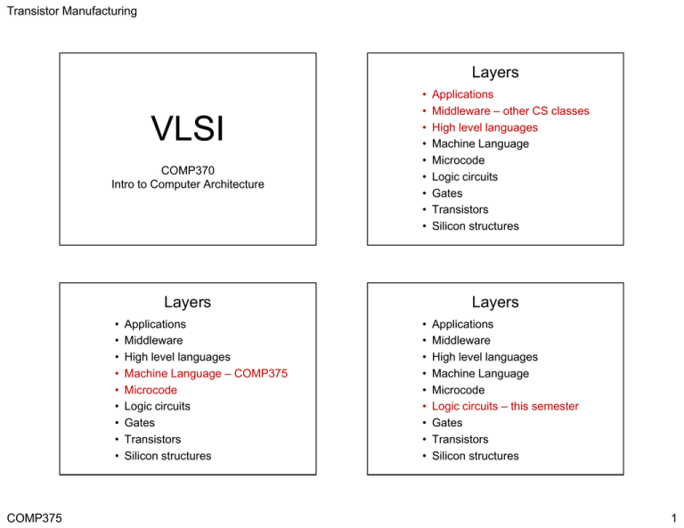
Transistor Manufacturing Layers VLSI COMP370 I t to Intro t Computer C t Architecture A hit t • • • • • • • • • Layers • • • • • • • • • COMP375 Applications Middleware High level languages Machine Language – COMP375 Microcode Logic g circuits Gates Transistors Silicon structures Applications Middleware – other CS classes High level languages Machine Language Microcode Logic g circuits Gates Transistors Silicon structures Layers • • • • • • • • • Applications Middleware High level languages Machine Language Microcode Logic g circuits – this semester Gates Transistors Silicon structures 1 Transistor Manufacturing Layers • • • • • • • • • Applications Middleware High level languages Machine Language Microcode Logic g circuits Gates – Earlier with more to come Transistors Silicon structures Periodic Table of Elements Layers • • • • • • • • • Applications Middleware High level languages Machine Language Microcode Logic g circuits Gates Transistors - Today Silicon structures Silicon • Silicon has a valance of 4 and is in the middle of its row in the periodic table. • Pure Silicon is a very poor conductor. • Phosphorus has one more electron than Silicon. It is a N type dopant. • Boron has one less electron than Silicon. I is It i an P type dopant. d • Adding just one part per million or less of a P dopant to silicon gives it extra electrons making it a good conductor. COMP375 2 Transistor Manufacturing n-channel MOS transistor Top View COMP375 NPN Transistor Operation Side View Metal good conductor for gates lightly P-doped silicon normally poor conductor heavily N-doped silicon good conductor Silicon Dioxide (glass) insulator The low concentration P type silicon is a poor conductor. Therefore very little current flows from the source to the gate. Transistor Operation PNP Transistor When positive voltage is applied to the gate, electrons are attracted to the gate. The presence of electrons allows current to flow between the source and drain. Infusing a lot of N dopant in an area makes a well of N doped silicon. A PNP transistor can be built in the well. 3 Transistor Manufacturing Complementary Operation • NPN transistors conducts electricity b t between the th source and dd drain i when h current is applied to the gate. • PNP transistors conducts electricity between the source and drain when no current is applied to the gate. They stop conducting when current is applied to the gate. • Complementary Metal Oxide Semiconductor i ad is design i ttechnique h i using i b both th NPN and d PNP transistors. • PNP transistors are used to connect the power to the output. • NPN transistors are used to connect the ground to the output. • The PNP and NPN circuits are exact logical inverses. NPN Transistor Stick Diagram PNP Transistor Stick Diagram Gate Gate Source Conducts when the gate has current. COMP375 CMOS Drain Source Drain Conducts when the gate does not have current. 4 Transistor Manufacturing Which Circuit Conducts? 1. cc 50% Size Considerations 50% 2. cg Gap 3. g gc 0% gc cg cc 0% gg 4. gg Capacitance The smaller the region of P type silicon between the source and the drain, the faster the transistor. Capacitance Factors Top View • Capacitance is a circuit’s ability to hold a charge. h • Greater capacitance increases the time required for a circuit to change voltage. • Increasing the width of the transistor elements increases the capacitance capacitance. Gate width Source width COMP375 5 Transistor Manufacturing Very Large Scale Integration • Transistors and the circuitry connecting th them is i built b ilt on a chip hi off silicon ili using i photolithography. • Millions of transistors can be manufactured on a single chip. Photoresist COMP375 VLSI Manufacturing Part 1 http://www.youtube.com/watch?v=tdkJ5Nn8oaM&feature=related p y Part 2 http://www.youtube.com/watch?v=UwT-HPCR5Gg&feature=related Part 3 http://www.youtube.com/watch?v=A70cW9jOZqc&feature=related Photolithography Etching 6 Transistor Manufacturing Photolithography Lift-off Projection Techniques What Does Photoresist Do? 1. Interconnects the circuits i it 2. Shields the silicon from chemicals 3. It is a dopant 4 Dissolves silicon 4. COMP375 7 Transistor Manufacturing Logic Gate Components •When the input is 1 (current) the upper PNP transistor does not conduct. Power cannot flow to the output Power Output Input Not Gate •The lower NPN transistor does conduct. The output is connected to ground. A A •When the input is 0 (no current) th upper PNP ttransistor the i t can conduct power to the output. •The lower NPN transistor does not connect the output to ground. Ground • When either A or B is 0, the output is connected to power. • When Wh both b th A and dB are one, the output is connected to ground. A 0 0 1 1 COMP375 B 0 1 0 1 NAND Gate CMOS NAND transistors output 1 1 1 0 8 Transistor Manufacturing • When A & B are 0, the output is connected to power. • When Wh either ith A or B are one, the output is connected to ground. A 0 0 1 1 B 0 1 0 1 NOR Gate output 1 0 0 0 Static RAM Cell Shorts • It is important that no combination of i inputs t connects t both b th the th power and d ground to the output. Power would flow from the power source to the ground creating a short and melting the chip. • The output should always be connected to either the power or the ground. Otherwise the output will “float”. CMOS Static RAM Bit • Draw the below gate diagram using only t transistors. i t COMP375 9 Transistor Manufacturing More Complex Example CMOS Carry Circuit • Consider the carry out equation for a one bit adder dd Cout = AB + BC + AC • The complement is Cout = (A+B)(B+C)(A+C) COMP375 10
