Pb Free Plating Product
ISSUED DATE :2005/03/02
REVISED DATE :2005/09/30B
GSC4435
BVDSS
RDS(ON)
ID
P-CHANNEL ENHANCEMENT MODE POWER MOSFET
-30V
20m
-8A
Description
The GSC4435 provide the designer with the best combination of fast switching, ruggedized device design, low
on-resistance and cost-effectiveness.
The SOP-8 package is universally preferred for all commercial-industrial surface mount applications and suited
for low voltage applications such as DC/DC converters.
Features
*Simple Drive Requirement
*Lower On-resistance
*Fast Switching
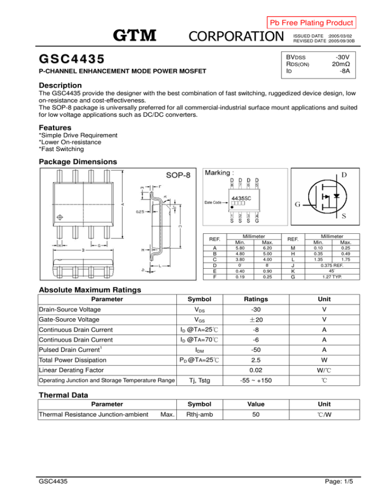
Package Dimensions
REF.
A
B
C
D
E
F
Millimeter
Min.
Max.
5.80
4.80
3.80
0
0.40
0.19
6.20
5.00
4.00
8
0.90
0.25
REF.
M
H
L
J
K
G
Millimeter
Min.
Max.
0.10
0.25
0.35
0.49
1.35
1.75
0.375 REF.
45
1.27 TYP.
Absolute Maximum Ratings
Parameter
Symbol
Ratings
Unit
Drain-Source Voltage
VDS
-30
V
Gate-Source Voltage
VGS
20
V
Continuous Drain Current
ID @TA=25
-8
A
Continuous Drain Current
ID @TA=70
-6
A
-50
A
2.5
W
Pulsed Drain Current
1
IDM
PD @TA=25
Total Power Dissipation
Linear Derating Factor
0.02
Operating Junction and Storage Temperature Range
Tj, Tstg
-55 ~ +150
Symbol
Value
Rthj-amb
50
W/
Thermal Data
Parameter
Thermal Resistance Junction-ambient
GSC4435
Max.
Unit
/W
Page: 1/5
ISSUED DATE :2005/03/02
REVISED DATE :2005/09/30B
Electrical Characteristics(Tj = 25
Parameter
Unless otherwise specified)
Symbol
Min.
Typ.
Max.
Unit
Drain-Source Breakdown Voltage
BVDSS
-30
-
-
V
Breakdown Voltage Temperature Coefficient
BVDSS / Tj
-
-0.037
-
Gate Threshold Voltage
VGS(th)
-1.0
-
-3.0
V
VDS=VGS, ID=-250uA
gfs
-
20
-
S
VDS=-10V, ID=-8A
IGSS
-
-
100
nA
VGS=
-
-
-1
uA
VDS=-30V, VGS=0
-
-
-5
uA
VDS=-24V, VGS=0
-
-
20
-
-
35
Forward Transconductance
Gate-Source Leakage Current
Drain-Source Leakage Current(Tj=25 )
Drain-Source Leakage Current(Tj=70 )
Static Drain-Source On-Resistance
IDSS
RDS(ON)
V/
m
Test Conditions
VGS=0, ID=-250uA
Reference to 25 , ID=-1mA
20V
VGS=-10V, ID=-8A
VGS=-4.5V, ID=-5A
Total Gate Charge2
Qg
-
47
-
Gate-Source Charge
Qgs
-
9.5
-
Gate-Drain (“Miller”) Change
Qgd
-
8
-
Td(on)
-
-
30
Tr
-
-
20
Td(off)
-
-
120
Tf
-
-
80
Input Capacitance
Ciss
-
-
2800
Output Capacitance
Coss
-
-
1400
Reverse Transfer Capacitance
Crss
-
-
350
Symbol
Min.
Typ.
Max.
Unit
VSD
-
-0.75
-1.2
V
IS=-2.1A, VGS=0V, Tj=25
IS
-
-
-2.1
A
VD=VG=0V, VS=-1.2V
ISM
-
-
-50
A
Turn-on Delay Time2
Rise Time
Turn-off Delay Time
Fall Time
nC
ID=-4.6A
VDS=-15V
VGS=-10V
ns
VDS=-15V
ID=-1A
VGS=-10V
RG=6
RD=15
pF
VGS=0V
VDS=-15V
f=1.0MHz
Source-Drain Diode
Parameter
2
Forward On Voltage
Continuous Source Current (Body Diode)
Pulsed Source Current (Body Diode)
1
Test Conditions
Notes: 1. Pulse width limited by safe operating area.
2. Pulse width 300us, duty cycle 2%.
GSC4435
Page: 2/5
ISSUED DATE :2005/03/02
REVISED DATE :2005/09/30B
Characteristics Curve
Fig 1. Typical Output Characteristics
Fig 2. Typical Output Characteristics
Fig 3. On-Resistance v.s. Gate Voltage
Fig 4. Normalized On-Resistance
v.s. Junction Temperature
Fig 5. Maximum Drain Current
v.s. Case Temperature
Fig 6. Type Power Dissipation
GSC4435
Page: 3/5
ISSUED DATE :2005/03/02
REVISED DATE :2005/09/30B
Fig 7. Maximum Safe Operating Area
Fig 9. Gate Charge Characteristics
Fig 11. Forward Characteristics of
Reverse Diode
GSC4435
Fig 8. Effective Transient Thermal Impedance
Fig 10. Typical Capacitance Characteristics
Fig 12. Gate Threshold Voltage v.s.
Junction Temperature
Page: 4/5
ISSUED DATE :2005/03/02
REVISED DATE :2005/09/30B
Fig 13. Switching Time Circuit
Fig 14. Switching Time Waveform
Fig 15. Gate Charge Circuit
Fig 16. Gate Charge Waveform
Important Notice:
All rights are reserved. Reproduction in whole or in part is prohibited without the prior written approval of GTM.
GTM reserves the right to make changes to its products without notice.
GTM semiconductor products are not warranted to be suitable for use in life-support Applications, or systems.
GTM assumes no liability for any consequence of customer product design, infringement of patents, or application assistance.
Head Office And Factory:
Taiwan: No. 17-1 Tatung Rd. Fu Kou Hsin-Chu Industrial Park, Hsin-Chu, Taiwan, R. O. C.
TEL : 886-3-597-7061 FAX : 886-3-597-9220, 597-0785
China: (201203) No.255, Jang-Jiang Tsai-Lueng RD. , Pu-Dung-Hsin District, Shang-Hai City, China
TEL : 86-21-5895-7671 ~ 4 FAX : 86-21-38950165
GSC4435
Page: 5/5
