ISSN: 2278 – 7798
International Journal of Science, Engineering and Technology Research (IJSETR)
Volume 5, Issue 8, August 2016
A Neutral Point Clamped Based Inverter for Three-Phase UPS
System Applications
S.NIRANJAN1, DR.B.RAMA KUMAR2
Abstract:
Uninterrupted Power Supply (UPS) system supplies
required power in case of utility power failures. UPS
system has got significant importance in the field of
industrial electronics due to increase in technology of
power electronic devices.This paper proposes a Neutral
Point Clamped (NPC) inverter with simple Sinusoidal
Pulse Width Modulation Technique (SPWM), which is
well suitable for inverter control. The proposed system
would be subjected to fast transient response, small
steady state error and low harmonic distortion test under
different load conditions. Finally, the comparative results
for the proposed scheme and the observer based voltage
control scheme are presented to show that the proposed
scheme achieves better performance. The results are
tested and verified through MATLAB/Simulink. The
proposed methodology reduces the total cost, complexity
and THD.
Keywords: Inverter, Uninterrupted Power Supply (UPS),
Neutral Point Clamped (NPC) Inverter, Three-Phase
Inverter, Total Harmonic Distortion (THD), SinusoidalPulse
Width Modulation (SPWM).
I.
and experimental results do not show better performance in
terms of steady-state error and THD. In [5], the deadbeat
control method uses the state feedback information to
compensate for the voltage drop across the inductor, but this
method is sensitive as parameter mismatches. FLC is
presented in [6]. This control strategy is proposed to
achieve low THD under nonlinear load. However, it is
complex due to computations. In [1], the observer based
voltage control method is proposed. This method achieved
better performance, but involves complex design.
Therefore, this paper proposes Neutral Point Clamped
(NPC) inverter with space vector modulation technique,
which is well suitable for inverter control. The proposed
system would be subjected to fast transient response, small
steady state error and low harmonic distortion test under
different load conditions. Finally, the comparative results for
the proposed schemend the observer based voltage control
scheme are presented to show that the proposed scheme
achieves better performance. The results would be tested and
verified through Matlab/Simulink. The proposed
methodology reduces the total cost, complexity and THD.
INTRODUCTION
Uninterrupted power supply (UPS) systems play a vital role
in case of utility power failures. It supplies emergency
power when power failure occurs. Recently the significance
of the UPS system has been increased more and more due to
increase of critical and sensitive applications like
telecommunication
systems,
medical
equipment,
manufacturing of semiconductor devices and data processing
systems. Such applications need high reliability and clean
power irrespective of the electric power failures and
distorted supply voltages. UPS system performance is
generally evaluated in terms of steady state /transient
response and total harmonic distortion of the output voltage
irrespective of load conditions like linear load, nonlinear
load and sudden load step change. To enhance the above
mentioned performance parameters, several control
strategies have been evolved such as adaptive control
method, proportional-integral (PI) control method, sliding
mode control scheme, model predictive control method,
feedback linearization control, deadbeat control method and
observer based voltage control method.
The conventional PI control method [2] and [3] is simple for
implementation but, the THD of the output voltage is not
reduced under nonlinear-load condition. A model predictive
control method is suggested in [4]. A load current observer
is used in place of current sensors, which resulted in the
reduction of overall system cost. However, the simulation
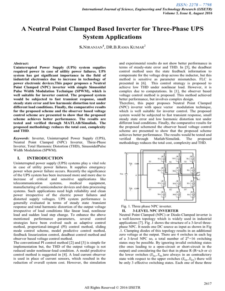
Fig. 1. Three phase NPC inverter.
II.
3-LEVEL NPC INVERTER
Neutral Point Clamped (NPC) or Diode-Clamped inverter is
a well-known topology which is widely used in industrial
applications [7]. Fig .1 shows the structure of a 3-level threephase NPC. It needs one DC source as input as shown in Fig
.1. Clamping diodes of this topology results in an additional
zero voltage at the output. There are 4 switches in each leg
of a 3-level NPC so, a total number of 24 =16 switching
states may be possible. By ignoring invalid switching states
(the ones leading to a open-circuit or short-circuit in the
output) and considering the fact that in phase R (R=a,b or c)
the lower switches (𝑆3𝑎 , 𝑆4𝑎 )are always in an contradictory
state with respect to the upper switches (𝑆1𝑎 , 𝑆2𝑎 ) there will
be only 3 effective switching states. Each one of these three
2617
All Rights Reserved © 2016 IJSETR
ISSN: 2278 – 7798
International Journal of Science, Engineering and Technology Research (IJSETR)
Volume 5, Issue 8, August 2016
states which aredenoted as 0, 1 and 2 and their respective
voltages in the output are given in Table I.
State ―1‖ gives a zero voltage by using clamping diodes to
connect the neutral point (O) to the output. In the similar
𝑣
𝑣
manner state ―2‖ (―0‖) gives + 𝑑𝑐 (- 𝑑𝑐 ) by applying voltage
2
2
of capacitor C1 (reverse voltage of C2) to the output. As an
illustration, Fig. 2 Shows how switching state ―2‖ generates
𝑣
a positive (+ 2𝑑𝑐 ) voltage at the phase output (𝑣𝑎𝑜 ). As
stated earlier, the only change between 3- level NPC and the
conventional 2- level full-bridge inverter is clamping diodes.
For each leg of an n- level NPC, there would be (𝑛 −
1)(𝑛 − 2) clamping diodes and there would be (𝑛 − 1)DClink capacitors. Since these capacitors didvide the input
voltage (𝑣𝑑𝑐 ) among themselves, nominal voltage rating of
each of them them would be Vdc/ (n-1) as well as that of
each switches. But in case of an n-level (𝑛 > 3) NPC
inverter, clamping diodes will have different voltage ratings
because different reverse voltages might be given to them
[8]. 3-level output waveform of this inverter gives high
quality output but switching technique is another factor that
has to be taken in to account.
TABLE I
SWITCHING STATES OF NPC INVERTER
Switching
S2a
S4a
states
S1a
S3a
2
On
On
Off
Off
Inverter
Terminal
Voltage
(Va)
Vdc/2
1
Off
On
On
Off
0
0
Off
Off
On
On
-Vdc/2
There are three main switching techniques:
1- Carrier-based methods, 2- Selective Harmonic
Modulation (SHE) and 3- Space-Vector Modulation (SVM).
In general, SVM method is superior and advanced when
compared to the other methods. In the following section a
generalized SVM technique has been proposed.
III.
SYSTEM CONFIGURATION
The proposed three level inverter with load consists of
voltage source inverter. The inverter model connected to the
load as shown in Fig 3. This is controlled to produce the
sinusoidal output. Three level SVPWM which is based on
orientation of reference point in terms of hexagon line is
proposed to lower the harmonic contents in the output
voltage.
(a)
Fig.3. Block diagram of the proposed NPC model.
(b)
Fig.2. Operating principle of three level NPC. (a)
Conducting path. (b). Corresponding output voltage.
Each leg of 3-level inverter have switching states of 0,1 or 2.
So, 27 switching states can be generated by this inverter.
Each one of these switching states can be denoted by a
number 𝑎𝑏𝑐 where 𝑎𝑏𝑐 ∈ {0,1,2} which is well explained in
[14]. Combination of some switches leads to identical
vectors known as redundant switching states. All 27
switching states results in producing only 19 different
voltage vectors due to redundant switching states. All the 19
voltage vectors and their respective switching states of a 3level NPC are represented in table II.
By using parks transformation three phase (abc) voltage
vectors is converted to two phase (αβ) plane. On connecting
these points a hexagram would be obtained which is SVM
diagram of 3-level NPC shown in Fig;4.
2618
All Rights Reserved © 2016 IJSETR
ISSN: 2278 – 7798
International Journal of Science, Engineering and Technology Research (IJSETR)
Volume 5, Issue 8, August 2016
TABLE II
THD(%) COMPARISON OF PROPOSED MODEL AND
EXISTING MODEL
Model
Step
Unbalanced
Nonlinear
change in
load
load
load
Observer
2.74
4.69
35.28
based
voltage
control
model
Proposed
1.57
1.59
8.25
model
IV.
CONTROL DESIGN OF THREE LEVEL
INVERTER
For industrial converters applications the sinusoidal PWM
technique is the most popular. In the general principle of
SPWM, a carrier wave of frequency fc is compared with the
fundamental frequency f sinusoidal modulating wave and
the points of intersection indicates the switching points of
power devices[9]. There are 8 switching states in the
traditional three phase two level inverter and there are 27
switches states in three level inverter. Three level pulse
width modulated waveforms can be produced by sine carrier
PWM. Sine carrier PWM is generated by comparing the
three reference control signals with two triangular carrier
waves [10] [11]. The block diagram of the proposed
controller is shown in Fig:4.
Fig:4. Block diagram of the controller
Fig.5. Simulation results of the proposed NPC model under
load step change —First: Load output voltages (𝑉𝐿 ), Second:
Load outputcurrents (𝐼𝐿 ).
Fig.6. Simulation results of the observer based voltage
control model under load step change —First: Load output
voltages (𝑉𝐿 ), Second: Load output currents (𝐼𝐿 ).
𝑉
𝑉𝑖𝑜 = 2𝑑𝑐 , 𝑉𝑟𝑒𝑓 , i>𝑉𝑡𝑟𝑖 ,1
=0, 𝑉𝑡𝑟𝑖 ,1>𝑉𝑟𝑒𝑓 , i>𝑉𝑡𝑟𝑖 , 2, where i = a, b or c
𝑉
= − 2𝑑𝑐 , 𝑉𝑡𝑟𝑖 , 2>𝑉𝑟𝑒𝑓 , i
The three reference control signals are in a phase shift of
1200 each other with same amplitude. Two carrier waves are
in phase each other with dc offset voltage.
.
V.
SIMULATION RESULTS AND DISCUSSION
Simulation was carried out with the help of ―MATLAB‖.
The proposed technique is carried out under different
conditions (i.e., load step change, unbalanced load, and
nonlinear load) to clearly represent its merits. The resistive
load is subjected to both the load step change condition and
the unbalanced load condition (i.e., phase B opened) to
check the capability of the proposed scheme when the load
is suddenly disconnected. To further test the robustness of
the proposed technique all load conditions such as load step
change, unbalanced load, and nonlinear load are considered.
Fig.7. Simulation results of the proposed NPC model under
unbalanced load (i.e., open phase) —First: Load output
voltages (𝑉𝐿 ), Second: Load output currents (𝐼𝐿 ).
2619
All Rights Reserved © 2016 IJSETR
ISSN: 2278 – 7798
International Journal of Science, Engineering and Technology Research (IJSETR)
Volume 5, Issue 8, August 2016
Fig.8. Simulation results of the observer based voltage
control model under unbalanced load (i.e., open phase) —
First: Load output voltages (𝑉𝐿 ), Second: Load output
currents (𝐼𝐿 ).
Fig. 5.Shows the simulation results of the proposed control
technique during the load step change andFig. 6. Presents
the comparative results obtained by employing the optimal
voltage control technique under the same condition.
Precisely, the figures display the load voltages (First
waveform:𝑽𝑳 ), load currents (Second waveform:𝑰𝑳 ). It can
be seen in Fig. 5 that when there is a sudden change in load,
the output voltage has little distortion. However, it returns to
a steady-state condition in 2.0 ms.On the other hand, as
shown in the simulation results in Fig. 6, current distortion is
longer as compared with that in Fig. 5. Also, the THD values
of the load output current at variousoperating conditions are
presented in Table II. These values are found as 2.74% for
observer based model and 1.57% usingthe proposed scheme.
Therefore, it is clearly stated that the proposed technique
attains lower THD.
.
Fig.10. Simulation results of the observer based voltage
control model under nonlinear load —First: Load output
voltages (𝑉𝐿 ), Second: Load output currents (𝐼𝐿 ).
The characteristic performances of the transient and steady
state under unbalanced load are tested through Figs. 7 and 8.
This case is implemented under a situation of full-load
condition by suddenly opening phase B. It is shown that the
output voltages are well controlled, although there is a rapid
change in the load current of phase B is observed as phase B
is opened. As shown in Fig. 7 and 8, the corresponding THD
values of the output currents are 4.69% for the observer
based model and 1.59% using the proposed method.
To estimate the steady-state performance in case of
nonlinear load, a three-phase diode rectifier is used. The
simulation results of both control methods under this
condition are shown in Figs. 9and 10. The THD values of
the load output current waveforms obtained with the
proposed scheme are 8.25% for proposed model and 35.28%
for observer based model, respectively. Finally, all THD
values under the three load conditions described earlier are
summarized in Table II.
VI.
CONCLUSION
This paper has proposed an NPC inverter with simple
SPWM for three-phase UPS system. The simulation of the
inverter was carried out using sinusoidal pulse width
modulation (SPWM). The performance of the proposed
control system was demonstrated through simulation under
various load conditions (load step change, unbalanced load
and nonlinear load). The proposed control scheme achieved
a better performance such as lower THD, small steady state
error and faster transient response.
REFERENCES
1.
Fig.9. Simulation results of the proposed NPC model under
nonlinear load —First: Load output voltages (𝑉𝐿 ), Second:
Load output currents (𝐼𝐿 ).
Eun-Kyung Kim, Francis Mwasilu, Han Ho Choi,
and Jin-Woo Jung ―An observer based optimal
voltage control scheme for three phase UPS
system,‖
IEEE
TRANSACTIONS
ON
INDUSTRIAL ELECTRONICS, VOL. 62, NO. 4,
APRIL 2015.
2620
All Rights Reserved © 2016 IJSETR
ISSN: 2278 – 7798
International Journal of Science, Engineering and Technology Research (IJSETR)
Volume 5, Issue 8, August 2016
2.
3.
4.
5.
6.
7.
8.
9.
10.
11.
12.
13.
U. Borup, P. N. Enjeti, and F. Blaabjerg, ―A new
space-vector-based control method for UPS
systems powering nonlinear and unbalanced loads,‖
IEEE Trans. Ind. Appl., vol. 37, no. 6, pp. 1864–
1870, Nov./Dec. 2001.
H. Karimi, A. Yazdani, and R. Iravani, ―Robust
control of an autonomous four-wire electronicallycoupled distributed generation unit,‖ IEEE
Trans.Power Del., vol. 26, no. 1, pp. 455–466, Jan.
2011.
P. Cortés et al., ―Model predictive control of an
inverter with output LC filter for UPS
applications,‖ IEEE Trans. Ind. Electron., vol. 56,
no. 6,pp. 1875–1883, Jun. 2009.
T. Kawabata, T. Miyashita, and Y. Yamamoto,
―Dead beat control of three phase PWM inverter,‖
IEEE Trans. Power Electron., vol. 5, no. 1, pp. 21–
28, Jan. 1990.
D. E. Kim and D. C. Lee, ―Feedback linearization
control of three-phase,‖ IEEE Trans. Ind. Electron.,
vol. 57, no. 3, pp. 963–968, Mar. 2010.
R. H. Baker, "Switching circuit," ed: Google
Patents, 1980.
J. Rodriguez, J.-S. Lai, and F. Z. Peng, "Multilevel
inverters: a survey of topologies, controls, and
applications,"
Industrial
Electronics,
IEEETransactions on, vol. 49, pp. 724-738, 2002.
Kapil Jain, Pradyumn Chaturvedi ―Matlab -based
Simulation & Analysis of Three - level SPWM
Inverter‖ International Journal of Soft Computing
and Engineering (IJSCE)ISSN: 2231-2307,
Volume-2, Issue-1, March 2012.
H. Vahedi and K. Al-Haddad, "Real-Time
Implementation of a Packed U-Cell Seven-Level
Inverter with Low Switching Frequency
VoltageRegulator," Power Electronics, IEEE
Transactions on, vol. PP, pp. 1-1, 2015.
P. Qashqai, A. Sheikholeslami, H. Vahedi, and K.
Al-Haddad, "A Review on Multilevel Converter
Topologies
for
Electric
Transportation
Applications,"
in
Vehicle
Power
and
PropulsionConference (VPPC), 2015 IEEE, 2015,
pp. 1-6.
Hamid R. Teymour, Kashem M. Muttaqi, “Solar
PV and Battery Storage Integration using a New
Configuration of a Three-Level NPC Inverter With
Advanced
Control
Strategy,‖IEEE
TRANSACTIONS ON ENERGY CONVERSION,
VOL. 29, NO. 2, JUNE 2014.
Xinbo Ruan, Bin Li, Qianhong Chen, Siew-Chong
Tan,”Fundamental Considerations of Three-Level
DC DC Converters: Topologies, Analyses, and
Control‖, IEEE TRANSACTIONS ON CIRCUITS AND
15. H. Tao, J. L. Duarte, andM. A.M. Hendrix, ―Lineinteractive UPS using afuel cell as the primary
source‖ IEEE TRANSACTIONS ON CIRCUITS AND
SYSTEMS—I: REGULAR PAPERS, VOL. 55, NO. 8, Aug
2008.
S. NIRANJAN received his B. Tech degree in electrical
engineering from the University of Vikrama Simhapuri in
2014. He is currently working towards the M.Tech degree.
DR. B. RAMA KUMAR received his B. Tech degree in
electrical engineering from The Institute of Engineers in
1994, received his M.Tech degree in electrical power
systems from the Institute of Advanced Studies in
Engineering in 2005, received his PhD. degree in solar
systems for silk industry from the University of JNTU
Anantapuramu in 2011. Presently he is working as Vice
Principal - Academics in MITS college, Madanapalle,
Andhra Pradesh.
SYSTEMS—I: REGULAR PAPERS, VOL. 55, NO. 11,
DECEMBER 2008.
14. Pouria Qashqai, Hani Vahedi,“A general space
vector nodulation technique for multilevel NPC
inverter‖ IEEE TRANSACTIONS ON CIRCUITS AND
SYSTEMS—I: REGULAR PAPERS, DECEMBER 2016.
2621
All Rights Reserved © 2016 IJSETR
