LN60A01
600V, Triple N-Channel MOSFET
with Common Gate Control
The Future of Analog IC Technology
DESCRIPTION
FEATURES
The LN60A01 is a three channel, 600V NChannel, enhancement mode power FET
manufactured in MPS's proprietary, highvoltage DMOS technology.
•
•
•
•
•
•
This advanced technology has been especially
tailored to minimize the on-state resistance,
provide superior switching performance, and
withstand high energy pulses in the avalanche
and commutation modes. This device is well
suited for high efficiency switched mode power
supplies and active power factor correction.
The LN60A01 is available in PDIP8 and SOIC8
package.
600V Breakdown Voltage
Three N-Channel MOSFETs
One Gate control to All Three FETs
Rds(on)=200Ω at Vgs=10V
Switching Current>0.1A
Fast Switching
APPLICATIONS
•
•
•
High Efficiency AC/DC Adaptor
Offline Switching Power Supply
Active Power Factor Correction
“MPS” and “The Future of Analog IC Technology” are Registered Trademarks
of Monolithic Power Systems, Inc.
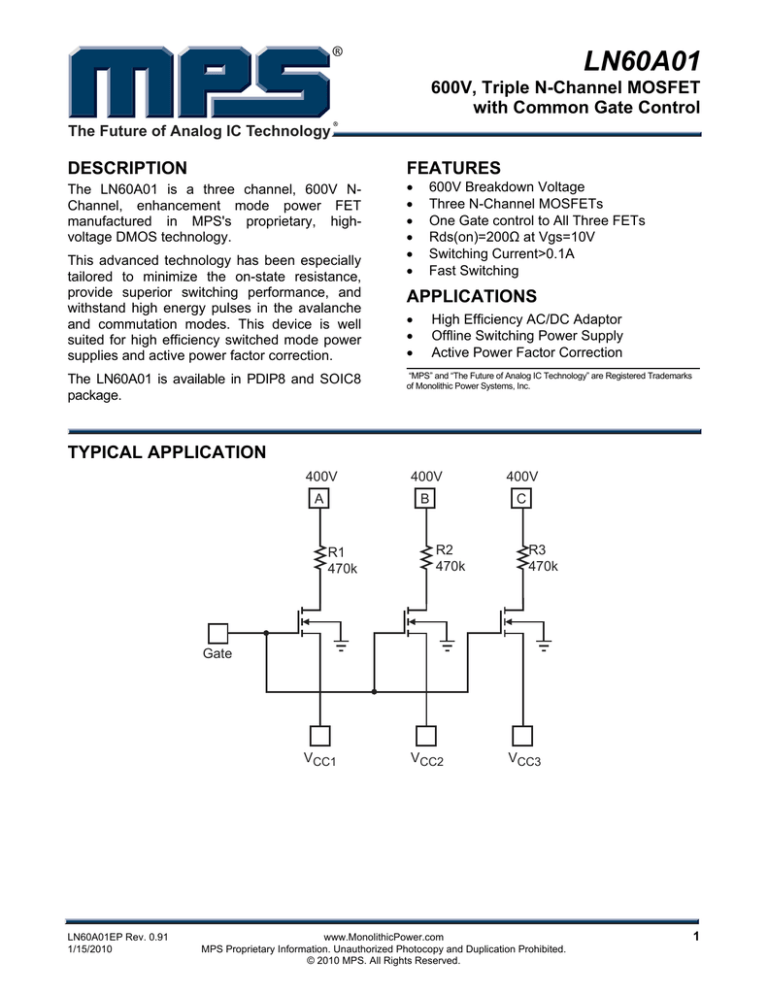
TYPICAL APPLICATION
400V
400V
400V
A
B
C
R1
470k
R2
470k
R3
470k
Gate
VCC1
LN60A01EP Rev. 0.91
1/15/2010
VCC2
VCC3
www.MonolithicPower.com
MPS Proprietary Information. Unauthorized Photocopy and Duplication Prohibited.
© 2010 MPS. All Rights Reserved.
1
LN60A01 – 600V, N-CHANNEL MOSFET
ORDERING INFORMATION
Part Number*
LN60A01EP
Part Number**
LN60A01ES
Package
PDIP-8
Package
SOIC-8
Free Air Temperature (TA)
-20ºC to 85ºC
Free Air Temperature (TA)
-20ºC to 85ºC
Top Marking
LN60A01E
Top Marking
LN60A01E
*For RoHS compliant packaging, add suffix –LF (e.g. LN60A01EP–LF)
** For Tape & Reel, add suffix –Z (e.g. LN60A01ES–Z).
For RoHS compliant packaging, add suffix –LF (e.g. LN60A01ES–LF–Z)
PACKAGE REFERENCE
TOP VIEW
TOP VIEW
S1
1
8
D1
S1
1
8
D1
S2
2
7
D2
S2
2
7
D2
Gate
3
6
D3
Gate
3
6
D3
S3
4
5
GND
S3
4
5
GND
PDIP-8
ABSOLUTE MAXIMUM RATINGS (1)
Drain-Source Voltage VDS .......................... 600V
Gate-Source Voltage VGS……………………..15V
Continuous Drain Current (1) ID .................. 0.08A
Pulsed Drain Current (2) IDM ......................... 0.4A
Power Dissipation (1) (2) PD .......................... 1.3W
Storage Temperature.............. –55°C to +150°C
LN60A01EP Rev. 0.91
1/15/2010
SOIC-8
Recommended Operating Conditions
Operating Junct. Temp (TJ)..... –20°C to +125°C
Thermal Resistance
(3)
θJA
θJC
SOIC8 ........................................90 ... 45... °C/W
PDIP8 ....................................105... . 45. .°C/W
Notes:
1) Surface Mounted on 1”×1” FR4 Board..
2) Pulse width limited by maximum junction temperature.
3) Measured on JESD51-7, 4-layer PCB
www.MonolithicPower.com
MPS Proprietary Information. Unauthorized Photocopy and Duplication Prohibited.
© 2010 MPS. All Rights Reserved.
2
LN60A01 – 600V, N-CHANNEL MOSFET
ELECTRICAL CHARACTERISTICS
TA = +25°C, unless otherwise noted.
Parameters
Symbol
Condition
V(BR)DSS
VGS=0V, ID=30uA
Min
Typ
Max
Units
Static Parameter
Drain-Source
Voltage
Breakdown
Gate Threshold Voltage
Zero Gate
Current
Voltage
Drain
Drain-Source On-Resistance
600
VGS(th)
VDS=VGS, ID=250uA
IDSS
VDS=400V, VGS=0V
15
VGS=10V, ID=10mA
190
VGS=5V, ID=10mA
200
rDS(on)
0.8
1.0
V
1.2
V
µA
Ω
Switching Parameter
Turn-On Delay Time
t(on)
Turn-Off Delay Time
t(off)
VDS=350V, IDS=10mA
50
3000
ns
PIN FUNCTIONS
Pin Number
Pin Name
1
S1
Source 1
2
3
4
5
6
7
8
S2
Gate
S3
GND
D3
D2
D1
Source 2
Gate
Source 3
Ground
Drain 3
Drain 2
Drain 1
LN60A01EP Rev. 0.91
1/15/2010
Description
www.MonolithicPower.com
MPS Proprietary Information. Unauthorized Photocopy and Duplication Prohibited.
© 2010 MPS. All Rights Reserved.
3
LN60A01 – 600V, N-CHANNEL MOSFET
DEVICE CIRCUIT
D1
D2
D3
GND
8
7
6
5
Q1
LN60A01EP Rev. 0.91
1/15/2010
Q2
Q3
1
2
3
4
S1
S2
GATE
S3
www.MonolithicPower.com
MPS Proprietary Information. Unauthorized Photocopy and Duplication Prohibited.
© 2010 MPS. All Rights Reserved.
4
LN60A01 – 600V, N-CHANNEL MOSFET
TYPICAL PERFORMANCE CHARACTERISTICS
TA =25ºC, unless otherwise noted.
RDS_ON vs. VGS
250
VGS_th vs. Temperature
IDS=5mA
1.4
VGS_th Voltage (V)
230
210
190
170
150
0
2
4
6
VGS (V)
8
10
IDS=250uA
380
1.2
330
1.0
280
0.8
230
0.6
180
0.4
130
0.2
-50
-20
10
40
70 100 130
Switching ON
Switching OFF
VDS=300V, IDS=4mA, VGS=5V
VDS=300V, IDS=4mA, VGS=5V
VGS
5V/div
VGS
5V/div
VDS
100V/div
VDS
100V/div
40ns/div
LN60A01EP Rev. 0.91
1/15/2010
RDS_ON vs. Temperature
VGS=10V, IDS=10mA
80
-50
-20
10
40
70 100 130
2us/div
www.MonolithicPower.com
MPS Proprietary Information. Unauthorized Photocopy and Duplication Prohibited.
© 2010 MPS. All Rights Reserved.
5
LN60A01 – 600V, N-CHANNEL MOSFET
PACKAGE INFORMATION
PDIP-8
0.367(9.32)
0.387(9.83)
8
5
0.240(6.10)
0.260(6.60)
PIN 1 ID
4
1
TOP VIEW
0.320( 8.13)
0.400(10.16)
0.300(7.62)
0.325(8.26)
0.100(2.54)
BSC
0.125(3.18)
0.145(3.68)
0.015(0.38)
0.035(0.89)
0.120(3.05)
0.140(3.56)
0.050(1.27)
0.065(1.65)
0.015(0.38)
0.021(0.53)
FRONT VIEW
0.008(0.20)
0.014(0.36)
SIDE VIEW
NOTE:
1) CONTROL DIMENSION IS IN INCHES. DIMENSION IN BRACKET IS IN MILLIMETERS.
2) PACKAGE LENGTH AND WIDTH DO NOT INCLUDE MOLD FLASH, OR PROTRUSIONS.
3) DRAWING CONFORMS TO JEDEC MS-001, VARIATION BA.
4) DRAWING IS NOT TO SCALE.
LN60A01EP Rev. 0.91
1/15/2010
www.MonolithicPower.com
MPS Proprietary Information. Unauthorized Photocopy and Duplication Prohibited.
© 2010 MPS. All Rights Reserved.
6
LN60A01 – 600V, N-CHANNEL MOSFET
PACKAGE INFORMATION
SOIC8
NOTICE: The information in this document is subject to change without notice. Please contact MPS for current specifications.
Users should warrant and guarantee that third party Intellectual Property rights are not infringed upon when integrating MPS
products into any application. MPS will not assume any legal responsibility for any said applications.
LN60A01EP Rev. 0.91
1/15/2010
www.MonolithicPower.com
MPS Proprietary Information. Unauthorized Photocopy and Duplication Prohibited.
© 2010 MPS. All Rights Reserved.
7


