VOL. 10, NO. 16, SEPTEMBER 2015
ISSN 1819-6608
ARPN Journal of Engineering and Applied Sciences
©2006-2015 Asian Research Publishing Network (ARPN). All rights reserved.
www.arpnjournals.com
MULTILEVEL INVERTER BASED ON LEVEL SWITCH AND H-BRIDGE
Sayat Moldakhmetov, Nalik Issembergenov and Abdurazak Kasymov
Kazakh National Technical University named after K.I. Satpayev, Almaty, Kazakhstan
E-Mail: sayatmoldakhmetov@gmail.com
ABSTRACT
This article proposes a topology for construction of multilevel inverter consisting of H-bridge and level switch. In
accordance with the proposed topology Н-bridge inverts voltage and a switch enables to get any number of voltage levels.
At that, in comparison with analogues, the above mentioned topology allows saving on expensive power keys. Moreover, a
special technique has been developed to set time of level switching. 13-level inverter has been developed following the
proposed topology and methodology. The article highlights the results of simulation in Matlab and an experimental inverter
unit.
Keywords: multilevel inverter, inverter topology, switching angles, THD.
INTRODUCTION
In modern power electronics multilevel inverter
development got a short in the arm with the appearance of
powerful IGBT modules. There are many different
methods for multilevel inverter construction. Most of them
are described in details in [1, 2]. The simplest multilevel
inverter topology is called “Cascaded Н-bridge” [3-5]. It
consists of several H-bridges in series which is not
economically beneficial because IGBT modules are rather
expensive. There is an improved topology with less power
elements [5, 6]. Diode clamped inverters or [7, 8] flying
capacitors [9] are also widely used. The topology
highlighted in the article [10] reduces a number of IGBT
used but such a topology requires more total supply
voltage and a complicated control system. The article
proposes construction topology for multilevel inverter
combining Н-bridge and level switch. At that, the level
switch enables to have any number of voltage levels at the
inverter output. There is also a methodology presented to
determine the switching time of inverter stages. It is based
on the geometrical approximation of voltage step curve to
sinusoidal wave.
METHODOLOGY FOR DETERMINING THE
SWITCHING TIME OF INVERTER STAGES
There are many ways to find switching time of
inverter voltage levels. Varieties of Shifting PWM [1, 2, 3]
are most often used. All of them are intended to
approximate step output voltage of inverter to sinusoidal
one and reduce its harmonic components. However, it is
not considered that such parameters of inverter output
voltage as frequency, amplitude and effective value should
conform to the parameters of industrial voltage. To
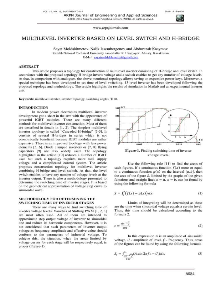
achieve this, the situation, when the areas limited by
voltage curves for each stage will be respectively equal, is
proper (Figure-1).
Figure-1. Finding switching time of inverter
voltage levels.
Use the following rule [11] to find the areas of
such figures. If a continuous function � more or equal
to a continuous function � on the interval [ , ], then
the area of the figure �, limited by the graphs of the given
functions and straight lines � = , � = , can be found by
using the following formula
�=∫ ( � −
� ) ��.
(1)
Limits of integrating will be determined as these
are the time when sinusoidal voltage equals a certain level.
Thus, this time should be calculated according to the
formula 2.
=
�
si − �
.
2��
(2)
In this expression � is an amplitude of sinusoidal
voltage, � - amplitude of level, - frequency. Thus, areas
of the figures can be found by using the following formula
�
�� = ∫sin� −
��
�
��
� �� 2�
− �� � ,
(3)
6884
VOL. 10, NO. 16, SEPTEMBER 2015
ISSN 1819-6608
ARPN Journal of Engineering and Applied Sciences
©2006-2015 Asian Research Publishing Network (ARPN). All rights reserved.
www.arpnjournals.com
�
sin− �ℎ
��
�ℎ = ∫�
�
�ℎ − � �� 2�
� .
(4)
The unknown time of switching falls within the
limits of integrating the given expressions. It is necessary
to extract integrals and make �� = �ℎ . As a result we get
the following
=
�
�
�
�
�ℎ si − ℎ −�� si − � +� c s si − ℎ −�c s si − �
�
�
2�� �ℎ −��
�
�
.
(5)
Thus, the formula has been obtained to find the
switching time of a certain voltage level.
SIMULATION AND EXPERIMENTAL RESULTS
In accordance with this formula we make a
practical calculation for a 13-level inverter. The inverter
topology is shown in Figure 2. Since the voltage will be
produced by 12 V accumulator batteries in series the
voltage levels should be divisible by 12. In this case they
are equal to 60, 120, 180, 240, 288 and 312 V respectively.
The obtained data are summarized in the Table-1.
Figure-2. 13-levels inverter circuit.
Table-1. Switching angles in 13-level inverter.
Level
1
2
3
4
5
6
Voltage, V
60
120
180
240
288
312
Switching time, s
Switching angles, deg
-3
-3
5.526° - 174.474°
-3
-3
16.794° - 163.206°
0.307·10 - 9.693·10
0.933·10 - 9.067·10
-3
1.6·10 - 8.4·10
-3
28.8° - 151.2°
-3
-3
42.462° - 137.538°
-3
-3
58.122° - 121.878°
-3
-3
74.952° - 105.048°
2.359·10 - 7.641·10
3.229·10 - 6.771·10
4.164·10 - 5.836·10
A six-level inverter has been simulated based on
the obtained results in Matlab software environment
(Figure-3). The parameters of inverter output voltage and
its harmonic composition were studied with the help of
powergui block.
Figure-3. 13-levels inverter model.
6885
VOL. 10, NO. 16, SEPTEMBER 2015
ISSN 1819-6608
ARPN Journal of Engineering and Applied Sciences
©2006-2015 Asian Research Publishing Network (ARPN). All rights reserved.
www.arpnjournals.com
The result of simulation is step voltage generation
at the inverter output. At 311.5 V amplitude an average
square value equals 220.2 V. The ratio of harmonic
distortion is 5.17% only which is a good result. For
example, the analogues ratio for 13-level inverter in [12,
13] according to HES-PSO-strategy is 6.11%. It has to be
recognized that in [14] THD less than 5% has been
obtained by using genetic algorithm. However, it should be
noted that in this case up to with respect to others shown
up 25th and 27th harmonics. They can easily be eliminated
by LC-filter.
Figure-6. Photograph of the experimental setup.
Figure-4. Simulation with MATLAB SIMULINK: output
voltage waveform of the 13-levels inverter.
After the scheme validation in MATLAB an
experimental unit was assembled. The Figure-5 shows a
structural scheme of inverter and the Figure-6 an
experimental unit. The inverter consists of a 6-channel
switch, a Н-bridge and a control system built on
microcontroller ATmega32A.
Н-bridge is made on the basis of intellectual
power module Mitsubishi PM75CLA120. It consists of
control impulse amplifier and protection scheme against
short circuit, current overload, low voltage or module high
temperature. In addition, it produces the “Emergency”
signal which is displayed by LEDs HL1, HL2 and HL3. To
ensure normal operation the module is optically coupled.
The module is powered from the DC source with voltage
of +15 V. The nominal power of the developed 13-level
inverter is 5 kWt.
Figure-5. Block diagram of the experimental unit.
Figure-7 shows an oscillogram of sinusoid shaped
output voltage of the inverter constructed according to the
switching angels in Table-1. This oscillogram also shows
voltage of industrial network of Almaty City for
comparison. As it can be noted the form of multilevel
inverter output voltage is more like sinusoidal than the
form of voltage in the industrial network.
Figure-7. Oscillogram of the 13-level inverter
output voltage.
CONCLUSIONS
This article proposed an alternative construction
topology for multilevel inverter. The topology can be used
to generate voltage of any number of levels. There was a
methodology for setting the switching time of levels and a
formula for quick calculation proposed. The 13-level
inverter was developed according to the proposed topology
and methodology for calculation of the switching time
which is rather good in relation to the THD and price. The
THD of the presented 13-level inverter turned out to be
less than the THD of analogue ones. The article presents
the scheme of constriction, simulation results and the
inverter experimental unit with the capacity of 5 kWt.
6886
VOL. 10, NO. 16, SEPTEMBER 2015
ISSN 1819-6608
ARPN Journal of Engineering and Applied Sciences
©2006-2015 Asian Research Publishing Network (ARPN). All rights reserved.
www.arpnjournals.com
REFERENCES
[1] J. Rodriguez, J.-S. Lai and F. Z. Peng. 2002.
Multilevel inverters: A survey of topologies,
controls, and applications. IEEE Trans. Ind. Electron.
49(4): 724-738.
[12] R. Taleb, A. Meroufel, A. Massoum. 2014. Control
of a Uniform Step Asymmetrical 13-Level Inverter
Using Particle Swarm Optimization. ATKAFF
Automatika. 55(1): 79-89.
[2] B. Singh, N. Mittal, and K. S. Verma. 2012. Multilevel inverter: A literature survey on topologies and
control strategies. International Journal of Reviews in
Computing. 10: 1-16.
[13] Espinosa E.E., Espinoza J.R., Melin P.E., Ramirez
R.O., Felipe Villarroel, Munoz J.A., Luis Moran.
2014. A New Modulation Method for a 13-Level
Asymmetric Inverter toward Minimum THD. IEEE
Transactions on Industry Applications. 50(3): 19241933.
[3] Arvind Yadav and Jagdish Kumar. 2013. Harmonic
Reduction in Cascaded Multilevel Inverter.
International Journal of Recent Technology and
Engineering. 2(2): 147-149.
[14] Debnath S., Narayan R. 2012. THD Optimization in
13 level photovoltaic inverter using Genetic
Algorithm. International Journal of Engineering
Research and Applications. 2(3): 385-389.
[4] Jagdish Kumar. 2012. THD Analysis for Different
Levels of Cascade Multilevel Inverters for Industrial
Applications. International Journal of Emerging
Technology and Advanced Engineering. 2(10): 237244.
[5] Bailu Xiao, Faete Filho and Tolbert L.M. 2011.
Single-Phase Cascaded H-Bridge Multilevel Inverter
with Non active Power Compensation for Grid
Connected
Photovoltaic
Generators.
Energy
Conversion Congress and Exposition. pp. 2733-2737.
[6] Rokan Ali Ahmed and S. Mekhilef. 2010. New
multilevel inverter topology with reduced number of
switches. IMEPCON.
[7] Xiaoming Yuan, Ivo Barbi. 2000. Fundamentals of a
New Diode Clamping Multilevel Inverter. IEEE
Transactions on Power Electronics. 15(4): 711-718.
[8] Zhiguo Pan, F. Z. Peng, Keith A. Corzine, Victor R.
Stefanovic, John M. Leuthen, and Slobodan Gataric.
2005. Voltage Balancing Control of Diode-Clamped
Multilevel Rectifier/Inverter Systems. IEEE Trans on
Industry Applications. 41(6): 1698-1706.
[9] Miguel F. Escalante, Jean-Claude Vannier, and Amir
Arzandé. 2002. Flying Capacitor Multilevel Inverters
and DTC Motor Drive Applications. IEEE Trans. On
Industrial Electronics. 49(4): 809-815.
[10] Ebrahim Babaei, Somayeh Alilu,and Sara Laali.
2014. A New General Topology for Cascaded
Multilevel Inverters with Reduced Number of
Components Based on Developed H-Bridge. IEEE
Transactions on Industrial Electronics. 61(8): 39323939.
[11] Chung S.K. 2014. Understanding Basic Calculus.
Create Space Independent Publishing Platform. pp.
173-175.
6887


