CA-3086
Data Sheet
December 15, 2011
FN483.6
General Purpose NPN Transistor Array
Applications
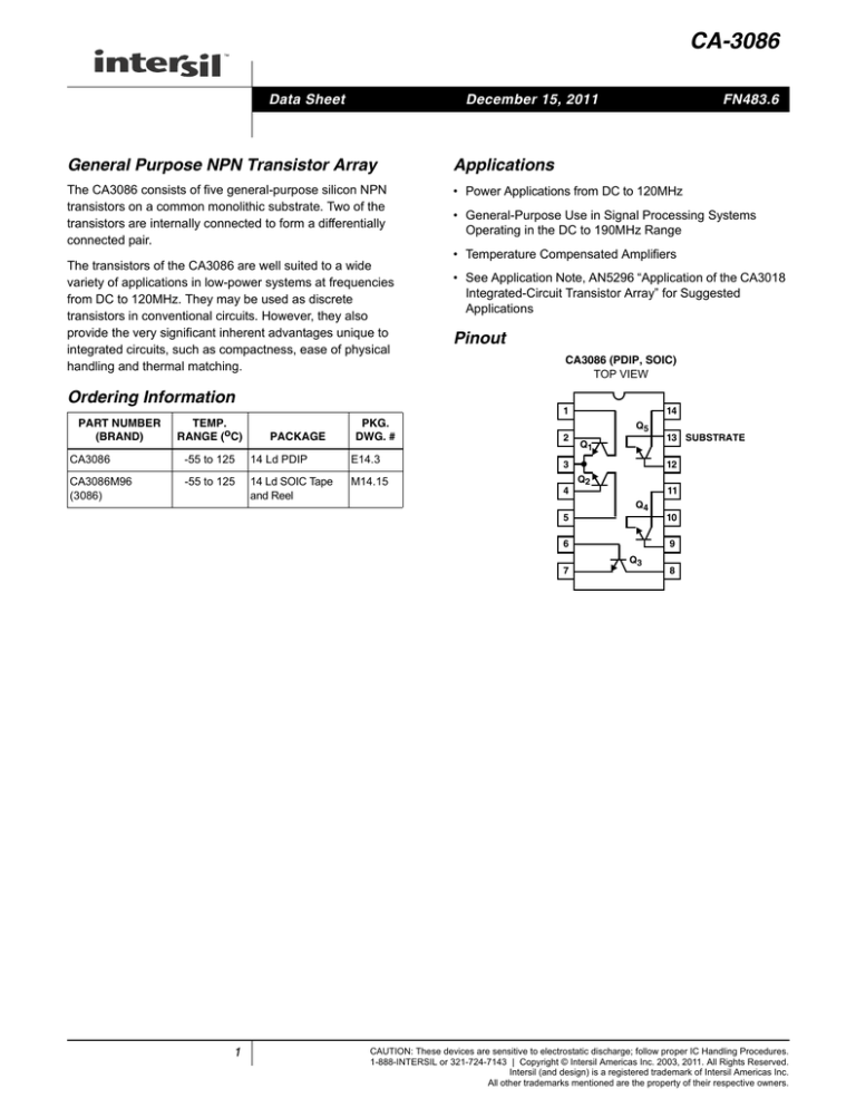
The CA3086 consists of five general-purpose silicon NPN
transistors on a common monolithic substrate. Two of the
transistors are internally connected to form a differentially
connected pair.
• Power Applications from DC to 120MHz
The transistors of the CA3086 are well suited to a wide
variety of applications in low-power systems at frequencies
from DC to 120MHz. They may be used as discrete
transistors in conventional circuits. However, they also
provide the very significant inherent advantages unique to
integrated circuits, such as compactness, ease of physical
handling and thermal matching.
Ordering Information
PART NUMBER
(BRAND)
TEMP.
RANGE (oC)
PACKAGE
PKG.
DWG. #
CA3086
-55 to 125
14 Ld PDIP
E14.3
CA3086M96
(3086)
-55 to 125
14 Ld SOIC Tape
and Reel
M14.15
• General-Purpose Use in Signal Processing Systems
Operating in the DC to 190MHz Range
• Temperature Compensated Amplifiers
• See Application Note, AN5296 “Application of the CA3018
Integrated-Circuit Transistor Array” for Suggested
Applications
Pinout
CA3086 (PDIP, SOIC)
TOP VIEW
1
2
14
Q5
Q1
3
4
5
12
Q2
11
Q4
6
7
1
13 SUBSTRATE
10
9
Q3
8
CAUTION: These devices are sensitive to electrostatic discharge; follow proper IC Handling Procedures.
1-888-INTERSIL or 321-724-7143 | Copyright © Intersil Americas Inc. 2003, 2011. All Rights Reserved.
Intersil (and design) is a registered trademark of Intersil Americas Inc.
All other trademarks mentioned are the property of their respective owners.
CA-3086
Absolute Maximum Ratings
Thermal Information
The following ratings apply for each transistor in the device:
Collector-to-Emitter Voltage, VCEO . . . . . . . . . . . . . . . . . . . . .15V
Collector-to-Base Voltage, VCBO . . . . . . . . . . . . . . . . . . . . . . .20V
Collector-to-Substrate Voltage, VCIO (Note 1) . . . . . . . . . . . . .20V
Emitter-to-Base Voltage, VEBO . . . . . . . . . . . . . . . . . . . . . . . . .5V
Collector Current, IC . . . . . . . . . . . . . . . . . . . . . . . . . . . . . . . 50mA
Thermal Resistance (Typical, Note 2)
θJA (oC/W)
θJC (oC/W)
PDIP Package . . . . . . . . . . . . . . . . . . .
110
N/A
SOIC Package . . . . . . . . . . . . . . . . . . .
130
N/A
Maximum Power Dissipation (Any one transistor) . . . . . . . . .300mW
Maximum Junction Temperature (Plastic Package) . . . . . . . .150oC
Maximum Storage Temperature Range . . . . . . . . . . -65oC to 150oC
Maximum Lead Temperature (Soldering 10s) . . . . . . . . . . . . 300oC
(SOIC - Lead Tips Only)
Operating Conditions
Temperature Range . . . . . . . . . . . . . . . . . . . . . . . . . -55oC to 125oC
CAUTION: Stresses above those listed in “Absolute Maximum Ratings” may cause permanent damage to the device. This is a stress only rating and operation of the
device at these or any other conditions above those indicated in the operational sections of this specification is not implied.
NOTES:
1. The collector of each transistor in the CA3086 is isolated from the substrate by an integral diode. The substrate (Terminal 13) must be connected
to the most negative point in the external circuit to maintain isolation between transistors and to provide for normal transistor action. To avoid
undesirable coupling between transistors, the substrate (Terminal 13) should be maintained at either DC or signal (AC) ground. A suitable
bypass capacitor can be used to establish a signal ground.
2. θJA is measured with the component mounted on an evaluation PC board in free air.
Electrical Specifications
TA = 25oC, For Equipment Design
PARAMETER
SYMBOL
TEST CONDITIONS
MIN
TYP
MAX
UNITS
Collector-to-Base Breakdown Voltage
V(BR)CBO
lC = 10μA, IE = 0
20
60
-
V
Collector-to-Emitter Breakdown Voltage
V(BR)CEO
IC = 1mA, IB = 0
15
24
-
V
Collector-to-Substrate Breakdown Voltage
V(BR)ClO
IC = 10μA, ICI = 0
20
60
-
V
Emitter-to-Base Breakdown Voltage
V(BR)EBO
IE = 10μA, IC = 0
5
7
-
V
Collector-Cutoff Current (Figure 1)
ICBO
VCB = 10V, IE = 0,
-
0.002
100
nA
Collector-Cutoff Current (Figure 2)
ICEO
VCE = 10V, IB = 0,
-
(Figure 2)
5
μA
DC Forward-Current Transfer Ratio (Figure 3)
hFE
VCE = 3V, IC = 1mA
40
100
-
Electrical Specifications
TA = 25oC, Typical Values Intended Only for Design Guidance
PARAMETER
SYMBOL
DC Forward-Current Transfer Ratio
(Figure 3)
hFE
Base-to-Emitter Voltage (Figure 4)
VBE
TEST CONDITIONS
VCE = 3V
VCE = 3V
TYPICAL
VALUES
UNITS
IC = 10mA
100
IC = 10μA
54
IE = 1 mA
0.715
V
IE = 10mA
0.800
V
VBE Temperature Coefficient (Figure 5)
ΔVBE/ΔT
VCE = 3V, lC = 1 mA
-1.9
mV/oC
Collector-to-Emitter
Saturation Voltage
VCE SAT
IB = 1mA, IC = 10mA
0.23
V
f = 1kHz, VCE = 3V, IC = 100μA,
RS = 1kΩ
3.25
dB
Noise Figure (Low Frequency)
NF
2
CA-3086
Electrical Specifications
TA = 25oC, Typical Values Intended Only for Design Guidance (Continued)
PARAMETER
SYMBOL
Low-Frequency, Small-Signal EquivalentCircuit Characteristics:
TEST CONDITIONS
TYPICAL
VALUES
UNITS
f = 1kHz,VCE = 3V, IC = 1mA
Forward Current-Transfer Ratio
(Figure 6)
hFE
100
-
Short-Circuit Input Impedance
(Figure 6)
hIE
3.5
kΩ
Open-Circuit Output Impedance
(Figure 6)
hOE
15.6
μS
Open-Circuit Reverse-Voltage
Transfer Ratio (Figure 6)
hRE
1.8 X 10⁻⁴
-
f = 1MHz,VCE = 3V, lC = 1mA
Admittance Characteristics:
Forward Transfer Admittance
(Figure 7)
yFE
31 - j1.5
mS
Input Admittance (Figure 8)
yIE
0.3 + j0.04
mS
Output Admittance (Figure 9)
yOE
0.001 + j0.03
mS
Reverse Transfer Admittance
(Figure 10)
yRE
See Figure 10
-
Gain-Bandwidth Product (Figure 11)
fT
VCE = 3V, IC = 3mA
550
MHz
Emitter-to-Base Capacitance
CEBO
VEB = 3V, IE = 0
0.6
pF
Collector-to-Base Capacitance
CCBO
VCB = 3V, IC = 0
0.58
pF
Collector-to-Substrate Capacitance
CClO
VC l = 3V, IC = 0
2.8
pF
Typical Performance Curves
103
IE = 0
10
COLLECTOR CUTOFF CURRENT (nA)
COLLECTOR CUTOFF CURRENT (nA)
102
VCB = 15V
VCB = 10V
VCB = 5V
1
10-1
10-2
10-3
10-4
0
25
50
75
100
TEMPERATURE (oC)
FIGURE 1. ICBO vs TEMPERATURE
3
125
IB = 0
102
VCE = 10V
10
VCE = 5V
1
10-1
10-2
10-3
0
25
50
75
TEMPERATURE (oC)
100
FIGURE 2. ICEO vs TEMPERATURE
125
CA-3086
Typical Performance Curves
0.8
VCE = 3V
TA = 25oC
110
BASE-TO-EMITTER VOLTAGE (V)
STATIC FORWARD CURRENT
TRANSFER RATIO (hFE)
120
(Continued)
hFE
100
90
80
70
60
0.1
1
0.7
VBE
0.6
0.5
0.4
0.01
50
0.01
VCE = 3V
TA = 25oC
10
0.1
EMITTER CURRENT (mA)
100
NORMALIZED h PARAMETERS
BASE-TO-EMITTER VOLTAGE (V)
VCB = 3V
0.9
0.8
0.7
IE = 3mA
IE = 1mA
IE = 0.5mA
0.5
0.4
-75
-50
-25
0
25
50
75
100
125
TEMPERATURE (oC)
hOE
hFE
hRE
hIE
0.1
0.01
6
INPUT CONDUCTANCE (gIE)
AND SUSCEPTANCE (bIE) (mS)
FORWARD TRANSFER CONDUCTANCE (gFE)
AND SUSCEPTANCE (bFE) (mS)
hIE
hRE
AT
1mA
0.1
1.0
COLLECTOR CURRENT (mA)
10
FIGURE 6. NORMALIZED hFE, hIE, hRE, hOE vs IC
30
gFE
10
0
bFE
-10
hFE = 100
hIE = 3.5kΩ
hRE = 1.88 x 10⁻⁴
hOE = 15.6μS
1.0
COMMON EMITTER CIRCUIT, BASE INPUT
TA = 25oC, VCE = 3V, IC = 1mA
20
VCE = 3V
f = 1kHz
TA = 25oC
10
FIGURE 5. VBE vs TEMPERATURE
40
10
FIGURE 4. VBE vs IE
FIGURE 3. hFE vs IE
0.6
1.0
EMITTER CURRENT (mA)
5
COMMON EMITTER CIRCUIT, BASE INPUT
TA = 25oC, VCE = 3V, IC = 1mA
4
3
bIE
2
gIE
1
0
-20
0.1
1
10
FREQUENCY (MHz)
FIGURE 7. yFE vs FREQUENCY
4
100
0.1
1
10
FREQUENCY (MHz)
FIGURE 8. yIE vs FREQUENCY
100
CA-3086
Typical Performance Curves
REVERSE TRANSFER CONDUCTANCE (gRE)
AND SUSCEPTANCE (bRE) (mS)
COMMON EMITTER CIRCUIT, BASE INPUT
TA = 25oC, VCE = 3V, IC = 1mA
5
4
bOE
3
2
1
gOE
0
0.1
1
10
FREQUENCY (MHz)
COMMON EMITTER CIRCUIT, BASE INPUT
TA = 25oC, VCE = 3V, IC = 1mA
gRE IS SMALL AT FREQUENCIES
LESS THAN 500MHz
0
bRE
-0.5
-1.0
-1.5
-2.0
100
1
FIGURE 9. yOE vs FREQUENCY
10
FREQUENCY (MHz)
FIGURE 10. yRE vs FREQUENCY
VCE = 3V
GAIN BANDWIDTH PRODUCT (MHz)
OUTPUT CONDUCTANCE (gOE)
AND SUSCEPTANCE (bOE) (mS)
6
(Continued)
TA = 25oC
1000
900
800
700
600
500
400
300
200
100
0
0
1
2
3
4
5
6
7
8
COLLECTOR CURRENT (mA)
FIGURE 11. fT vs IC
5
9
10
100
CA-3086
Dual-In-Line Plastic Packages (PDIP)
E14.3 (JEDEC MS-001-AA ISSUE D)
N
14 LEAD DUAL-IN-LINE PLASTIC PACKAGE
E1
INDEX
AREA
1 2 3
INCHES
N/2
-B-
-AD
E
BASE
PLANE
-C-
SEATING
PLANE
A2
A
L
D1
e
B1
D1
A1
eC
B
0.010 (0.25) M
C A B S
MILLIMETERS
SYMBOL
MIN
MAX
MIN
MAX
NOTES
A
-
0.210
-
5.33
4
A1
0.015
-
0.39
-
4
A2
0.115
0.195
2.93
4.95
-
B
0.014
0.022
0.356
0.558
-
C
L
B1
0.045
0.070
1.15
1.77
8
eA
C
0.008
0.014
C
D
0.735
0.775
18.66
eB
NOTES:
1. Controlling Dimensions: INCH. In case of conflict between English
and Metric dimensions, the inch dimensions control.
0.005
-
0.13
-
5
0.300
0.325
7.62
8.25
6
E1
0.240
0.280
6.10
7.11
5
e
0.100 BSC
eA
0.300 BSC
eB
-
L
0.115
4. Dimensions A, A1 and L are measured with the package seated in
JEDEC seating plane gauge GS-3.
N
8. B1 maximum dimensions do not include dambar protrusions. Dambar
protrusions shall not exceed 0.010 inch (0.25mm).
9. N is the maximum number of terminal positions.
10. Corner leads (1, N, N/2 and N/2 + 1) for E8.3, E16.3, E18.3, E28.3,
E42.6 will have a B1 dimension of 0.030 - 0.045 inch (0.76 1.14mm).
6
5
E
2. Dimensioning and tolerancing per ANSI Y14.5M-1982.
7. eB and eC are measured at the lead tips with the leads unconstrained. eC must be zero or greater.
0.355
19.68
D1
3. Symbols are defined in the “MO Series Symbol List” in Section 2.2 of
Publication No. 95.
5. D, D1, and E1 dimensions do not include mold flash or protrusions.
Mold flash or protrusions shall not exceed 0.010 inch (0.25mm).
6. E and eA are measured with the leads constrained to be perpendicular to datum -C- .
0.204
14
2.54 BSC
7.62 BSC
0.430
-
0.150
2.93
14
6
10.92
7
3.81
4
9
Rev. 0 12/93
CA-3086
Small Outline Plastic Packages (SOIC)
M14.15 (JEDEC MS-012-AB ISSUE C)
N
INDEX
AREA
0.25(0.010) M
H
14 LEAD NARROW BODY SMALL OUTLINE PLASTIC
PACKAGE
B M
E
INCHES
-B-
1
2
3
L
SEATING PLANE
-A-
h x 45o
A
D
-C-
e
µα
A1
B
0.25(0.010) M
C A M
SYMBOL
MIN
MAX
MIN
MAX
NOTES
A
0.0532
0.0688
1.35
1.75
-
A1
0.0040
0.0098
0.10
0.25
-
B
0.013
0.020
0.33
0.51
9
C
0.0075
0.0098
0.19
0.25
-
D
0.3367
0.3444
8.55
8.75
3
E
0.1497
0.1574
3.80
4.00
4
e
C
0.10(0.004)
B S
0.050 BSC
1. Symbols are defined in the “MO Series Symbol List” in Section 2.2 of
Publication Number 95.
1.27 BSC
-
H
0.2284
0.2440
5.80
6.20
-
h
0.0099
0.0196
0.25
0.50
5
L
0.016
0.050
0.40
1.27
6
N
NOTES:
MILLIMETERS
α
14
0o
14
8o
0o
7
8o
Rev. 0 12/93
2. Dimensioning and tolerancing per ANSI Y14.5M-1982.
3. Dimension “D” does not include mold flash, protrusions or gate burrs.
Mold flash, protrusion and gate burrs shall not exceed 0.15mm (0.006
inch) per side.
4. Dimension “E” does not include interlead flash or protrusions. Interlead
flash and protrusions shall not exceed 0.25mm (0.010 inch) per side.
5. The chamfer on the body is optional. If it is not present, a visual index
feature must be located within the crosshatched area.
6. “L” is the length of terminal for soldering to a substrate.
7. “N” is the number of terminal positions.
8. Terminal numbers are shown for reference only.
9. The lead width “B”, as measured 0.36mm (0.014 inch) or greater
above the seating plane, shall not exceed a maximum value of
0.61mm (0.024 inch).
10. Controlling dimension: MILLIMETER. Converted inch dimensions
are not necessarily exact.
All Intersil U.S. products are manufactured, assembled and tested utilizing ISO9000 quality systems.
Intersil Corporation’s quality certifications can be viewed at www.intersil.com/design/quality
Intersil products are sold by description only. Intersil Corporation reserves the right to make changes in circuit design, software and/or specifications at any time without
notice. Accordingly, the reader is cautioned to verify that data sheets are current before placing orders. Information furnished by Intersil is believed to be accurate and
reliable. However, no responsibility is assumed by Intersil or its subsidiaries for its use; nor for any infringements of patents or other rights of third parties which may result
from its use. No license is granted by implication or otherwise under any patent or patent rights of Intersil or its subsidiaries.
For information regarding Intersil Corporation and its products, see www.intersil.com
7
