ISL8010 Monolithic DC/DC Evaluation Board
Setup Procedure
®
Application Note
September 1, 2005
AN1205.0
Author: Steve Laur
Description
Ordering Information
This document describes the setup procedure for the
ISL8010EVAL1 Rev A board.
PART
NUMBER
The General Purpose market requires maximum flexibility in
its power management solutions due to the large variety of
applications produced each year. The ISL8010 services this
need by offering a multitude of functionality, combined with
features that allow it to work in many different application
spaces.
From a functional standpoint, the ISL8010 is an ideal
controller for designers that want a “plug and play” solution.
It delivers a regulated output voltage from 0.8V to 5.5V at a
maximum current of 600mA, with 10 or fewer total
components. Its 10 Ld MSOP package, combined with
integrated MOSFET switches and compensation, yield a
solution size below 0.18in2. This small form factor makes the
ISL8010 a desirable solution for any application where board
space is a premium (PDAs, cell phones, etc.).
Additional features include a power good (PG) indicator for
output voltage monitoring, and a clock frequency
synchronizing input (SYNC). The SYNC input allows the
regulator to switch anywhere between the nominal 1.4MHz
frequency and 12MHz. Synchronizing multiple switching
devices on the same bus eliminates beat-frequency
oscillations that can be detrimental to noise-sensitive
applications.
In battery supplied applications, where efficiency is most
important, the ISL8010 employs a pulse-frequency
modulation (PFM) mode to boost light-load efficiency
significantly over synchronous rectifiers. The controller will
automatically switch between PFM and PWM mode
depending on load conditions, or if PWM is always desired,
the SYNC pin can be used as a logic input to select this
state. Additional power saving is achieved when the ISL8010
is shut-down, sinking <1µA of stand-by current.
Overall, the ISL8010 delivers a robust, highly integrated
DC/DC buck converter for a variety of General Purpose
applications. For a more detailed description of the ISL8010,
refer to the data sheet [1].
The Intersil General Purpose family of monolithic switching
power supplies continues to expand with new selections to
better fit our customer’s needs.
1. Refer to our website for updated information and the ISL8010
data sheet: www.intersil.com.
1
PACKAGE
TAPE & REEL
PKG. DWG. #
ISL8010IUZ
10 Ld MSOP
-
MDP0043
ISL8010IUZ-T7
10 Ld MSOP
7”
MDP0043
ISL8010IUZ-T13
10 Ld MSOP
13”
MDP0043
NOTE: Intersil Pb-free plus anneal products employ special Pb-free
material sets; molding compounds/die attach materials and 100% matte
tin plate termination finish, which are RoHS compliant and compatible
with both SnPb and Pb-free soldering operations. Intersil Pb-free
products are MSL classified at Pb-free peak reflow temperatures that
meet or exceed the Pb-free requirements of IPC/JEDEC J STD-020.
Features
• Less than 0.18in2 Footprint for the Complete 600mA
Converter
• Components on One Side of PCB
• Max Height 1.1mm MSOP10
• Power-Good (PG) Output
• Internally-Compensated Voltage Mode Controller
• Up to 95% Efficiency
• <1µA Shut-Down Current
• 120µA Quiescent Current
• Hiccup Mode Overcurrent and Over-Temperature
Protection
• External Synchronization up to 12MHz
• Pb-Free Plus Anneal Available (RoHS Compliant)
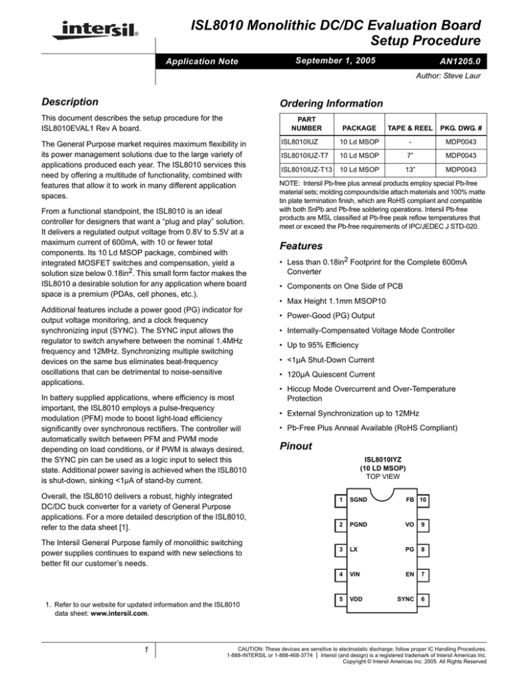
Pinout
ISL8010IYZ
(10 LD MSOP)
TOP VIEW
1
SGND
FB 10
2
PGND
VO
9
3
LX
PG
8
4
VIN
EN
7
5
VDD
SYNC
6
CAUTION: These devices are sensitive to electrostatic discharge; follow proper IC Handling Procedures.
1-888-INTERSIL or 1-888-468-3774 | Intersil (and design) is a registered trademark of Intersil Americas Inc.
Copyright © Intersil Americas Inc. 2005. All Rights Reserved
Application Note 1205
What’s Inside
TABLE 1. DETAILED DESCRIPTION OF SWITCH SETTINGS
The Evaluation Board Kit contains the following materials:
SWITCH
POSITION
FUNCTION
S1
ON
ENABLE ISL8010
OFF (default)
DISABLE ISL8010
• The ISL8010EVAL1 Rev A Evaluation Board
• The ISL8010 Data Sheet
• The ISL8010 Evaluation Board Setup Procedure (this
document)
What is Needed
TABLE 2. DETAILED DESCRIPTION OF TEST POINTS
REF DES
TYPE
FUNCTION
P1
Test Point
SYNC Input:
HIGH = Force PWM
LOW = Auto PFM/PWM
Switching = Clock Sync
• Precision Digital Multimeters
P2
Test Point
GND
• Oscilloscope
P3
Test Point
PGOOD Voltage
P6
Test Point
External Enable NOT. S1 is required
to be in the ON position.
J1
Oscilloscope
Kelvin LX Measurement
J2
Oscilloscope
Kelvin VOUT Measurement
P4
Binding Post
GND
P5
Binding Post
VIN
P7
Binding Post
VOUT
P8
Binding Post
GND
The following materials will be needed to perform testing:
• 1 Electronic Load (See Note)
• 1 Power Supply: 0-6V @ 2A (See Note)
NOTE: amperage rating of power supplies and loads are determined
by maximum expected loading plus a percentage margin of error.
Quick Setup Guide
Step 1:
Set the +VIN power supply to +3.3V and place in
the “STANDBY” or “OFF” position. Connect the
positive terminal (+) of the supply to the VIN
terminal P5 and the negative terminal (-) of the
supply to GND P4.
Step 2:
Connect the positive terminal (+) of a DMM to the
VIN terminal P5 and the negative terminal (-) to the
GND terminal P4.
Step 3:
Connect the positive terminal (+) of the electronic
load to the VOUT terminal P7. Connect the
negative terminal (-) of the electronic load to the
GND terminal P8. Make sure the electronic load is
set to the 0A condition.
Step 4:
Connect the positive terminal (+) of a DMM to the
VOUT terminal P7 and the negative terminal (-) to
the GND terminal P8.
Step 5:
Check to ensure all jumpers and switches are in
their default positions prior to application of power
(refer to Table 1: “DETAILED DESCRIPTION OF
SWITCH SETTINGS” ).
Step 6:
Set all power supplies to the “ON” position. LED D1
should be off. Check all DMM displays for correct
voltage levels. Adjust if necessary.
Step 7:
Turn the ENABLE switch S1 to the “ON” position.
LED D1 should glow red. The VOUT DMM should
read 1.80V (±5%).
At this point the board has been properly powered up.
Normal testing can begin.
EVAL Board Information
FIGURE 1. ISL8010EVAL1 REV A EVALUATION BOARD
NOTE: If you need technical assistance, or other assistance, with
the ISL8010 Evaluation Board, call 1-888-INTERSIL (468-3774).
2
AN1205.0
September 1, 2005
Application Note 1205
Eval Board Schematic
Z
3
AN1205.0
September 1, 2005
TABLE 3. BILL OF MATERIALS
ITEM
QTY
REFERENCE
VALUE
TYPE
1
1
U1
2
2
J1, J2
Tekronix Scope Jack
3
2
Q1, Q2
N-Channel MOSFET: 2N7002
4
1
C1, C2
10µF
Generic ceramic capacitor
1206
6.3V
5
2
C3
1µF
Generic ceramic capacitor
0603
6.3V
6
1
C4
4700pF
Generic ceramic capacitor
0603
6.3V
7
1
L1
1.8µH
8
1
S1
9
1
R1
124kΩ
Generic thick film chip resistor
0603
10
1
R2
100kΩ
Generic thick film chip resistor
0603
11
3
R3, R7, R8
1kΩ
Generic thick film chip resistor
0603
12
1
R4
10kΩ
Generic thick film chip resistor
0603
13
1
R5
750Ω
Generic thick film chip resistor
0603
14
1
R6
100Ω
Generic thick film chip resistor
0603
15
1
D1
Liteon: LTST-C170CKT
0603
16
4
P1, P2, P3, P6
Test Points
17
4
P4, P5, P7, P8
Binding Posts
Intersil ISL8010
FOOTPRINT
VOLTAGE
MSOP10
SOT-23
Coilcraft: 1008PS-182M
SPDT Switch: GT11MSCKE
Eval Board Layout
FIGURE 2. EVAL BOARD TOP LAYER ROUTING (ETCH)
FIGURE 3. EVAL BOARD BOTTOM LAYER ROUTING (ETCH)
All Intersil U.S. products are manufactured, assembled and tested utilizing ISO9000 quality systems.
Intersil Corporation’s quality certifications can be viewed at www.intersil.com/design/quality
Intersil products are sold by description only. Intersil Corporation reserves the right to make changes in circuit design, software and/or specifications at any time without
notice. Accordingly, the reader is cautioned to verify that data sheets are current before placing orders. Information furnished by Intersil is believed to be accurate and
reliable. However, no responsibility is assumed by Intersil or its subsidiaries for its use; nor for any infringements of patents or other rights of third parties which may result
from its use. No license is granted by implication or otherwise under any patent or patent rights of Intersil or its subsidiaries.
For information regarding Intersil Corporation and its products, see www.intersil.com
4
AN1205.0
September 1, 2005
