HS-303RH
TM
Data Sheet
November 2001
Radiation Hardened
CMOS Dual SPDT Analog Switch
• QML, Per MIL-PRF-38535
• Radiation Performance
- Gamma Dose (γ) 1 x 10⁵ RAD(Si)
• No Latch-Up, Dielectrically Isolated Device Islands
• Pin for Pin Compatible with Intersil HI-303 Series Analog
Switches
• Analog Signal Range 15V
• Low Leakage . . . . . . . . . . . . . . . . 100nA (Max, Post Rad)
• Low rON . . . . . . . . . . . . . . . . . . . . . . 60Ω (Max, Post Rad)
• Low Operating Power . . . . . . . . . . 100µA (Max, Post Rad)
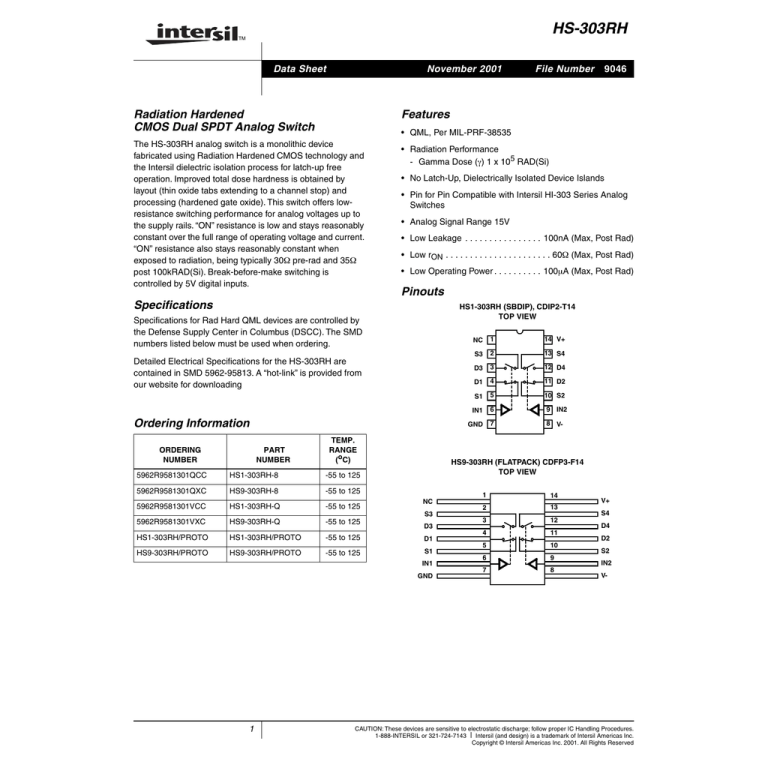
Pinouts
Specifications
HS1-303RH (SBDIP), CDIP2-T14
TOP VIEW
Specifications for Rad Hard QML devices are controlled by
the Defense Supply Center in Columbus (DSCC). The SMD
numbers listed below must be used when ordering.
Detailed Electrical Specifications for the HS-303RH are
contained in SMD 5962-95813. A “hot-link” is provided from
our website for downloading
Ordering Information
PART
NUMBER
TEMP.
RANGE
(oC)
HS1-303RH-8
-55 to 125
5962R9581301QXC
HS9-303RH-8
-55 to 125
5962R9581301VCC
HS1-303RH-Q
-55 to 125
5962R9581301VXC
HS9-303RH-Q
-55 to 125
HS1-303RH/PROTO
HS1-303RH/PROTO
-55 to 125
D1
-55 to 125
S1
NC
S3
HS9-303RH/PROTO
D3
IN1
GND
1
NC
1
14 V+
S3
2
13 S4
D3
3
12 D4
D1
4
11 D2
S1
5
10 S2
IN1
6
9 IN2
GND
7
8 V-
HS9-303RH (FLATPACK) CDFP3-F14
TOP VIEW
5962R9581301QCC
HS9-303RH/PROTO
9046
Features
The HS-303RH analog switch is a monolithic device
fabricated using Radiation Hardened CMOS technology and
the Intersil dielectric isolation process for latch-up free
operation. Improved total dose hardness is obtained by
layout (thin oxide tabs extending to a channel stop) and
processing (hardened gate oxide). This switch offers lowresistance switching performance for analog voltages up to
the supply rails. “ON” resistance is low and stays reasonably
constant over the full range of operating voltage and current.
“ON” resistance also stays reasonably constant when
exposed to radiation, being typically 30Ω pre-rad and 35Ω
post 100kRAD(Si). Break-before-make switching is
controlled by 5V digital inputs.
ORDERING
NUMBER
File Number
1
14
2
13
3
12
4
11
5
10
6
9
7
8
V+
S4
D4
D2
S2
IN2
V-
CAUTION: These devices are sensitive to electrostatic discharge; follow proper IC Handling Procedures.
1-888-INTERSIL or 321-724-7143 | Intersil (and design) is a trademark of Intersil Americas Inc.
Copyright © Intersil Americas Inc. 2001. All Rights Reserved
HS-303RH
Functional Diagram
SBDIP TRUTH TABLE
N
IN
P
D
LOGIC
SW1AND SW2
SW3 AND SW4
0
OFF
ON
1
ON
OFF
Die Characteristics
DIE DIMENSIONS:
PASSIVATION:
(2130µm x 1930µm x 279µm ±25.4µm)
84 x 76 x 11mils ±1mil
Type: Silox (SiO2)
Thickness: 8kÅ ±1kÅ
WORST CASE CURRENT DENSITY:
METALLIZATION:
< 2.0e5 A/cm2
Type: Al
Thickness: 12.5kÅ ±2kÅ
TRANSISTOR COUNT:
SUBSTRATE POTENTIAL:
76
Unbiased (DI)
PROCESS:
BACKSIDE FINISH:
Metal Gate CMOS, Dielectric Isolation
Gold
Metallization Mask Layout
S4
S3
V+
HS-303RH-T
D2
S1
S2
IN1
IN2
V-
D1
GND
D4
NC
D3
All Intersil products are manufactured, assembled and tested utilizing ISO9000 quality systems.
Intersil Corporation’s quality certifications can be viewed at www.intersil.com/design/quality
Intersil products are sold by description only. Intersil Corporation reserves the right to make changes in circuit design, software and/or specifications at any time without
notice. Accordingly, the reader is cautioned to verify that data sheets are current before placing orders. Information furnished by Intersil is believed to be accurate and
reliable. However, no responsibility is assumed by Intersil or its subsidiaries for its use; nor for any infringements of patents or other rights of third parties which may result
from its use. No license is granted by implication or otherwise under any patent or patent rights of Intersil or its subsidiaries.
For information regarding Intersil Corporation and its products, see www.intersil.com
2
