V3205 4096-Stage Low-Noise BBD Analog Delay Line
advertisement
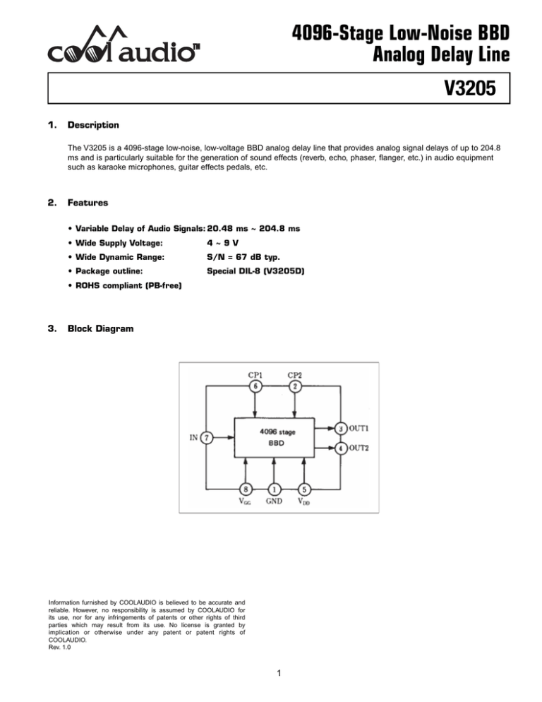
4096-Stage Low-Noise BBD Analog Delay Line V3205 1. Description The V3205 is a 4096-stage low-noise, low-voltage BBD analog delay line that provides analog signal delays of up to 204.8 ms and is particularly suitable for the generation of sound effects (reverb, echo, phaser, flanger, etc.) in audio equipment such as karaoke microphones, guitar effects pedals, etc. 2. Features • Variable Delay of Audio Signals: 20.48 ms ~ 204.8 ms • Wide Supply Voltage: 4~9V • Wide Dynamic Range: S/N = 67 dB typ. • Package outline: Special DIL-8 (V3205D) • ROHS compliant (PB-free) 3. Block Diagram Information furnished by COOLAUDIO is believed to be accurate and reliable. However, no responsibility is assumed by COOLAUDIO for its use, nor for any infringements of patents or other rights of third parties which may result from its use. No license is granted by implication or otherwise under any patent or patent rights of COOLAUDIO. Rev. 1.0 1 V3205 4. Pin Configuration 5. Circuit Diagram 6. Quick Reference Data Item Symbol Value Unit Supply Voltage VDD, VGG +5, 14/15VDD V Signal Delay Time tD 20.48 ~ 204.8 ms Total Harmonic Distortion THD 0.8 % Signal to Noise Ratio S/N 67 dB 2 V3205 7. 8. 9. Absolute Maximum Ratings (Ta=250C) Item Symbol Rating Unit Terminal Voltage VDD, VGG, VCP, Vi -0.3 ~ +11 V Output Voltage VO -0.3 ~ +11 Operation Ambient Temp. Topr Storage Temp. Tstg V -20 ~ +60 o -55 ~ +125 o C C Operating Conditions (Ta=250C) Item Symbol Condition Min Typ. Max Unit Drain Supply Voltage VDD +4 +5 +9 V Gate Supply Voltage VGG 14/ V 15 DD V Clock Voltage High VCPH VDD V Clock Voltage Low VCPL 0 +0.5 V Clock frequency fCP 10 100 KHz Clock Pulse Width *1 tCPW 0.5T*2 Clock Rise Time *1 tCPr 500 ns Clock fall Time *1 tCPf 500 ns Clock Input Capatence CCP 2800 pF Clock Cross Point VX 0.3VCPH V 0 Electrical Characteristics (Ta = 250C, VDD = VCPH = 5V, VCPL = 0V, VGG = 14/15 VDD, RL=100k ) Parameter Symbol Signal Delay Time tO Input Signal Frequency fi Input Signal Swing Vi Insertion Loss Li TotalHarmonic Distortion THD Output Noise Voltage VoN Signal to Noise Ratio S/N Condition Min Typ. 20.48 fCP = 40kHz, Max Unit 204.8 ms 6 kHz THD = 2.5% 0.36 Vrms fCP = 40kHz, fI = 1kHz -4 Output Attenuation ≤3dB fCP = 40kHz, fI = 1kHz, Vi = 0.25 Vrms 0 4 dB 0.8 2.5 % 0.35 mVrms tCP = 100 kHz, Weighted by “A” curve 3 67 dB V3205 * 1 Clock Pulse Waveform *2 T = 1/fCP (Clock Period) 10. Application Circuit 4 V3205 11. Mechanical Specifications unit : mm 5


