CHT-OPAL DATASHEET High-Temperature, Ultra High
advertisement

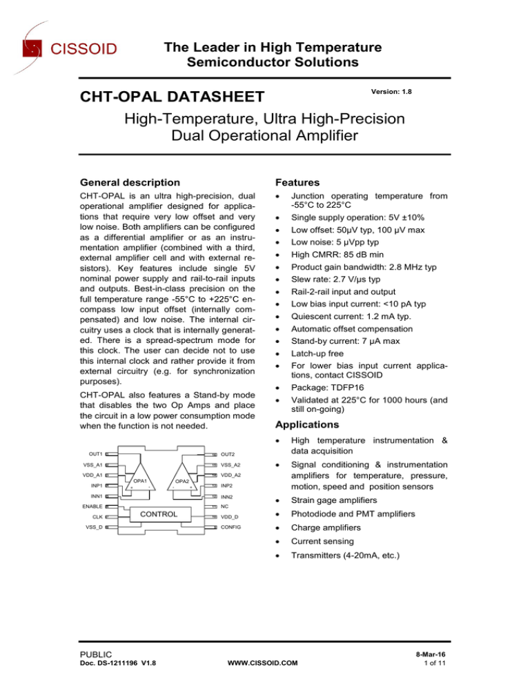
The Leader in High Temperature Semiconductor Solutions Version: 1.8 CHT-OPAL DATASHEET High-Temperature, Ultra High-Precision Dual Operational Amplifier General description Features CHT-OPAL is an ultra high-precision, dual operational amplifier designed for applications that require very low offset and very low noise. Both amplifiers can be configured as a differential amplifier or as an instrumentation amplifier (combined with a third, external amplifier cell and with external resistors). Key features include single 5V nominal power supply and rail-to-rail inputs and outputs. Best-in-class precision on the full temperature range -55°C to +225°C encompass low input offset (internally compensated) and low noise. The internal circuitry uses a clock that is internally generated. There is a spread-spectrum mode for this clock. The user can decide not to use this internal clock and rather provide it from external circuitry (e.g. for synchronization purposes). Junction operating temperature from -55°C to 225°C Single supply operation: 5V ±10% Low offset: 50µV typ, 100 µV max Low noise: 5 µVpp typ High CMRR: 85 dB min Product gain bandwidth: 2.8 MHz typ Slew rate: 2.7 V/µs typ Rail-2-rail input and output Low bias input current: <10 pA typ Quiescent current: 1.2 mA typ. Automatic offset compensation Stand-by current: 7 µA max Latch-up free For lower bias input current applications, contact CISSOID Package: TDFP16 CHT-OPAL also features a Stand-by mode that disables the two Op Amps and place the circuit in a low power consumption mode when the function is not needed. Validated at 225°C for 1000 hours (and still on-going) OUT1 1 16 OUT2 VSS_A1 2 15 VSS_A2 VDD_A1 3 14 VDD_A2 INP1 4 13 INP2 INN1 5 12 INN2 ENABLE 6 11 NC CLK 7 10 VDD_D VSS_D 8 OPA1 CONTROL + - + - OPA2 9 CONFIG Applications High temperature instrumentation & data acquisition Signal conditioning & instrumentation amplifiers for temperature, pressure, motion, speed and position sensors Strain gage amplifiers Photodiode and PMT amplifiers Charge amplifiers Current sensing Transmitters (4-20mA, etc.) PUBLIC Doc. DS-1211196 V1.8 WWW.CISSOID.COM 8-Mar-16 1 of 11 CHT-OPAL–DATASHEET Pinout VSS_A1 OUT1 OUT2 VSS_A1 VSS_A2 VDD_A1 VDD_A2 INP1 INP2 INN1 INN2 ENABLE NC CLK VDD_D VSS_D CONFIG VSS_A1 Pin # Pin Name Pin Description 1 OUT1 2 VSS_A1 Negative power supply Analog OPA1 3 VDD_A1 Positive power supply Analog OPA1 4 INP1 Positive input pin OPA1 5 INN1 Negative input pin OPA1 6 ENABLE Enable input pin 7 CLK Input clock signal 8 VSS_D 9 CONFIG Configuration input pin 10 VDD_D Positive power supply digital part 11 NC 12 INN2 Negative input pin OPA2 13 INP2 Positive input pin OPA2 14 VDD_A2 Positive power supply Analog OPA2 15 VSS_A2 Negative power supply Analog OPA2 16 OUT2 Output OPA1 1 1 Negative power supply digital part 1 Not connected Output OPA2 The 2 vertical large leads are internally connected to VSS_A1 and are also connected to the package heat sink. 1 Cfr “Mode of operations” for details about function of pins “CLK”, “CONFIG” and “ENABLE” PUBLIC Doc. DS-1211196 V1.8 WWW.CISSOID.COM 8-Mar-16 2 of 11 CHT-OPAL–DATASHEET Absolute Maximum Ratings Operating Conditions VDD_X – VSS_X VSS_X – VSS_Y VDD_X – VDD_Y Voltage on any pin wrt to VSS_X Junction Temperature (Tj) Supply Voltage VDD_X to VSS_X: Junction temperature -0.5 to 6V max 0.5V max 0.5V -0.5 to VDD_X+0.5V 250°C 4.5V to 5.5V -55°C to +225°C ESD Rating Human Body Model >2KV CAUTION: Stresses above those listed in “Absolute Maximum Ratings” may cause permanent damage to the device. This is a stress only rating and operation of the device at these or any other conditions above those indicated in the operational sections of this specification is not implied. Frequent or extended exposure to absolute maximum rating conditions or above may affect device reliability. Permanent uses of the device in short-circuit state or in over-temperature state may affect long term reliability of the device. PUBLIC Doc. DS-1211196 V1.8 WWW.CISSOID.COM 8-Mar-16 3 of 11 CHT-OPAL–DATASHEET DC Electrical Characteristics Unless otherwise stated, Tj = 25°C, VDD_D/VDD_A1/VDD_A2=5V. Bold figures point out values valid over the whole temperature range (Tj = -55°C to +225°C). Parameter Supply Voltage Output voltage range Symbol VDD_X – VSS_X VOUT Quiescent current IQ Standby current ISTDBY Internal clock frequency Output voltage swing FINT VO Max Output current1,2 IO Output short-circuit current ISC Condition Min 4.5 0 CLK= ‘0’; CONFIG= ‘0’ 1 amplifier active, no load CLK= ‘0’; CONFIG= ‘0’, ENABLE = ’0’; Tj = 25°C CLK= ‘0’; CONFIG= ‘0’, ENABLE = ’0’; Tj = 225°C CLK= ‘0’; CONFIG= ‘0’; Tj = 25°C Typ 5 1.2 VCM Input offset voltage VIOFF Input offset drift TCVIOFF Input leakage current IB Input offset current IOFF CIN,DIFF Input capacitance CIN,CM Open-loop output impedance Thermal resistance 1 2 θJC θJA Unit 2 mA 1.5 0.35 RL=1k 0.09 RL=∞ 0.01 Tj=25°C 20 Tj=225°C 15 kHz VDD -0.4 VDD -0.1 VDD 0.01 V V V mA mA 100 mA 200 VDD -0.1 0.1 Tj=25°C V µA 360 RL=250 V µA 7 External output capacitance Common mode input range Max 5.5 5 50 pF V µV 100 µV 90 µV Tj=225°C Maximum variation over [40-175]°C temperature range Tj=25°C, CMInput = 2.5V ±7 pA Tj=225°C, CMInput = 2.5V ±50 nA Tj=25°C ±14 pA Tj=225°C Differential, CMInput = 2.5V Single-ended, CMInput = 2.5V Io=0mA, f=3MHz, Av=+1 ±120 nA 1.5 pF 3 pF pad area = 1 cm2 150 250 400 Ω 11 °C/W 80 °C/W Source or sink. Output current is not internally limited. Value given indicates the maximum recommended conditions. PUBLIC Doc. DS-1211196 V1.8 WWW.CISSOID.COM 8-Mar-16 4 of 11 CHT-OPAL–DATASHEET AC Electrical Characteristics Unless otherwise stated, Tj = 25°C, VDD_D/VDD_A1/VDD_A2=5V. Bold figures point out values valid over the whole temperature range (Tj = -55°C to +225°C). Parameter Symbol DC open-loop gain AO Gain-bandwidth product Common mode rejection ratio Power supply rejection ratio GBW CMRR PSRR Slew rate SR Phase margin M Input noise spectral density Integrated input noise voltage Input noise current esd eni Condition RL=2k, Tj=25°C, CMInput = 2.5V RL=2k, Tj=225°C CMInput = 2.5V RL=2k, CL=30pF, Tj=25°C CMInput = 2.5V RL=2k, CL=30pF, Tj=225°C CMInput = 2.5V DC to 1kHz, Tj=25°C Min DC to 1kHz, Tj=225°C Positive or negative. DC to 100Hz, Tj=25°C CMInput = 2.5V Positive or negative. DC to 100Hz, Tj=225°C CMInput = 2.5V RL=2k, CL=30pF, Tj=25°C 1.9 2.7 RL=2k, CL=30pF, Tj=225°C 3 4 RL=2k, CL=30pF, Tj=25°C 35 41 ° RL=2k, CL=30pF, Tj=225°C 27 32 ° 85 dB 2.2 2.8 MHz 2.5 3.6 MHz 85 105 dB 88 99 dB 95 dB 95 dB F=100Hz 0.3 F=1kHz 0.3 F=10kHz 0.09 10Hz WWW.CISSOID.COM Unit dB 0.3 0.1 Hz to 10Hz Max 85 F=10Hz PUBLIC Doc. DS-1211196 V1.8 Typ V/µs µV/√ Hz 5 µVpp TBD fA/√H z 8-Mar-16 5 of 11 CHT-OPAL–DATASHEET Typical Performance Characteristics 12 14 VCM 1V 10 VCM 2V VCM 3V 8 10 VCM 3V VCM 4V Population Population VCM 1V 12 VCM 2V 6 VCM 4V 8 6 4 4 2 2 0 0 -80 -70 -60 -50 -40 -30 -20 -10 0 10 -10 20 0 10 20 30 40 50 60 70 80 90 100 Offset Voltage [uV] Offset Voltage [uV] Input Offset maximum thermal drift over (VCM= Input common mode voltage) [-40°C-175°C] temperature range (VDD=5V) 6.00E-12 6.00E-08 4.00E-12 5.00E-08 Iinput leakage current [A] Iinput leakage current [A] Input Offset distribution (VDD=5V, T=25°C) 2.00E-12 0.00E+00 -2.00E-12 -4.00E-12 4.00E-08 3.00E-08 2.00E-08 1.00E-08 0.00E+00 -6.00E-12 -1.00E-08 -8.00E-12 0.5 1 1.5 2 2.5 3 3.5 4 4.5 5 0.5 Input common mode voltage [V] Input leakage current vs input common mode voltage (25°C) 1.5 2 2.5 3 3.5 Input common mode voltage [V] 4 4.5 5 Input leakage current vs input common mode voltage (225°C) 2 100 1.8 90 1.6 Quiescent current [mA] 80 70 AOL (dB) 1 60 50 1.4 1.2 40 -55°C 30 25 °C 20 175°C 0.4 10 225°C 0.2 0 -55°C 25°C 1 125°C 0.8 175°C 0.6 225°C 0 10 100 1000 10000 0 100000 Frequency (Hz) Open loop Gain vs Frequency (no load) 2 3 Output Voltage [V] 4 5 Supply current vs temperature PUBLIC Doc. DS-1211196 V1.8 1 WWW.CISSOID.COM 8-Mar-16 6 of 11 CHT-OPAL–DATASHEET 120 PSRR (dB) 100 80 60 40 20 0 100 1000 10000 100000 Frequency (Hz) Large signal transient response (swing= 1V,gain =5, Cl= 220pF) PSRR vs Frequency Small signal transient response (swing= 100mV,gain =5, Cl= 220pF) Voltage noise Density from 0.1Hz to 20 KHz (purple: with compensation; yellow: without compensation) (real value = measured value – 60dB) Voltage noise Density from 0.1Hz to 1 KHz (purple: with compensation; yellow: without compensation) (real value = measured value – 60dB) PUBLIC Doc. DS-1211196 V1.8 WWW.CISSOID.COM 8-Mar-16 7 of 11 CHT-OPAL–DATASHEET Circuit Functionality Architecture CHT-OPAL implements two low-noise, low-offset operational amplifier cells. The amplifiers implement a proprietary compensation architecture for automatic offset correction and low-frequency noise improvement on the whole temperature range. As the use of a compensation clock generates unavoidable clock ripple on the output signal, and even though special care has been taken to the circuit design in order to minimize this ripple, the user may need to filter it externally. CHT-OPAL offers several configuration options in order to bring maximum flexibility to the user in regards to filtering: The clock operation can implement a spread spectrum function, which allows minimization of the output ripple amplitude on the clock frequency, the noise (ripple) energy being spread on the harmonics. Alternatively, the spread spectrum function can be disabled, in which case 100% of the ripple will be concentrated on the clock frequency. This later option is more suitable when external filtering (notch filter) or synchronization with external sampling devices is implemented. Secondly, OPAL’s offset compensation block can run either from an internal clock or from an external clock; the latter allows external synchronization and will typically be used by sampled systems (e.g. ADC). Use of the internal clock operation does not require any dedicated external components (e.g. capacitance). Selection of the external clock frequency can be made within a very wide range of 12 KHz to 500 KHz: the user will find an adequate frequency outside the useful bandwidth in most instrumentation and sensing applications. sumption mode, with only a few µA drawn from the power supply. External gain setting CHT-OPAL is intrinsically stable for gain higher 3V/V. For gain lower than 3V/V, an external compensation network should be added. The network shown on Figure 1 stabilizes CHT-OPAL in unitary gain configuration and reduces its bandwidth by a factor 6. Table below summarizes the different gain configurations. Gain (G) [V/V] G>5 3<G<5 G<3 Max output capacitance 200pF 50pF 50pF External compensation network Not needed Not needed Needed as shown on Figure 1 Figure 1 CHT-OPAL can also support higher output capacitance, with additional compensation network. Contact CISSOID for more information. When the spread spectrum function is enabled, CHT-OPAL compensation circuitry operates with a pseudo-random clock (generated from the master internal or external clock). This pseudo-random clock is generated by a 32-to-64 divider of the master clock (5.5 KHz to 11 KHz typ. When generated from the internal clock). This spreads the clock noise over a frequency octave. CHT-OPAL also features a shutdown mode where the 2 Op Amps are inactive; the circuit is then in its lowest power con- PUBLIC Doc. DS-1211196 V1.8 WWW.CISSOID.COM 8-Mar-16 8 of 11 CHT-OPAL–DATASHEET Modes of operation OPAL’s behavior is controlled by 3 configuration pins. Table1 below summarizes the 5 different modes of operation. Choice of one of those 4 modes depends on the application constraints (signal useful band, synchronization with external devices…). Single OPA CLK CONFIG ENABLE MODE OPERATION X X 0 MODE1 Standby mode 0 0 1 MODE2 Internal oscillator;spreadspectrum enabled CLK > 9kHz 0 1 MODE3 External clock;spreadspectrum enabled 1 0 1 Internal test mode 0 1 1 MODE4 Internal oscillator;spreadspectrum disabled CLK > 9kHz 1 1 MODE5 External clock;spreadspectrum disabled 1 1 X Internal test mode If the application only requires a single operational amplifier, the OPAL current consumption can be optimized by connecting VDD_A1 or VDD_A2 to respectively VSS_A1 or VSS_A2. MODE1: By setting the pin ENABLE to “0”, OPAL is put in standby mode where current consumption is reduced to a few µA. When OPAL is in that mode, the 2 outputs are in High Impedance state. MODE[2..5]: Those 4 modes are standard modes of operation for OPAL. They differ by the way the internal auto-zero control signals are internally generated. If CLK pin is put to “0”, the master clock is generated by an internal oscillator (Fosc = 360 KHz typ.). Whenever OPAL’ internal circuitry senses an external clock signal with a frequency higher than 9KHz applied on the CLK pin, the circuits operates automatically in external clock mode, using CLK signal as the master clock. With the CONFIG pin, one can configure OPAL to use the spread spectrum function to generate the internal auto-zero control signals PUBLIC Doc. DS-1211196 V1.8 WWW.CISSOID.COM 8-Mar-16 9 of 11 CHT-OPAL–DATASHEET Package Dimensions (TDFP16) 3.20 1.2 0.18 0.15 0.89 2.80 3.90 2.80 Min 6.00 / Max 6.50 0.635 0.5-0.75 5.00 5.50 0.18 7.50 Max Physical dimensions (mm +/- 10%) Ordering Information Product Name CHT-OPAL Ordering Reference CHT-GEM6489A-TDFP16-T PUBLIC Doc. DS-1211196 V1.8 WWW.CISSOID.COM Package TDFP16 Marking CHT-GEM6489A 8-Mar-16 10 of 11 CHT-OPAL–DATASHEET Contact & Ordering CISSOID S.A. Headquarters and contact EMEA: CISSOID S.A. – Rue Francqui, 3 – 1435 Mont Saint Guibert - Belgium T : +32 10 48 92 10 – F : +32 10 88 98 75 Email : sales@cissoid.com Sales Representatives: Visit our website: http://www.cissoid.com Disclaimer Neither CISSOID, nor any of its directors, employees or affiliates make any representations or extend any warranties of any kind, either express or implied, including but not limited to warranties of merchantability, fitness for a particular purpose, and the absence of latent or other defects, whether or not discoverable. In no event shall CISSOID, its directors, employees and affiliates be liable for direct, indirect, special, incidental or consequential damages of any kind arising out of the use of its circuits and their documentation, even if they have been advised of the possibility of such a damage. The circuits are provided “as is”. CISSOID has no obligation to provide maintenance, support, updates, or modifications. PUBLIC Doc. DS-1211196 V1.8 WWW.CISSOID.COM 8-Mar-16 11 of 11


