uClamp0541Z2A
01005 Size µClamp®
1-Line ESD Protection
PROTECTION PRODUCTS
Description
Features
µClamp® TVS diodes are designed to protect sensitive
electronics from damage or latch-up due to ESD. They
are designed to replace 01005 size multilayer varistors
(MLVs) in portable applications such as cell phones,
notebook computers, and other portable electronics. TVS diodes offer desirable characteristics for board level
protection including fast response time, low operating
and clamping voltage, and no device degradation.
• High ESD withstand voltage: +/-15kV (contact) and
+/-15kV (air)per IEC 61000-4-2
• Ultra-small 01005 package
• Protects one line
• Low ESD clamping voltage
• Working voltage: 5V
• Capacitance: 6.5pF Typical
• Low leakage current
• Low dynamic resistance
• Solid-state silicon-avalanche technology
µClamp®0541Z2A features extremely good ESD
protection characteristics highlighted by low dynamic
resistance, low peak ESD clamping voltage, and high
ESD withstand voltage (+/-15kV contact per IEC 61000-42). Low typical capacitance (6.5pF at VR=0V) minimizes
loading on sensitive cirucuits. Each device will protect
one data or power line operating at 5 Volts.
Mechanical Characteristics
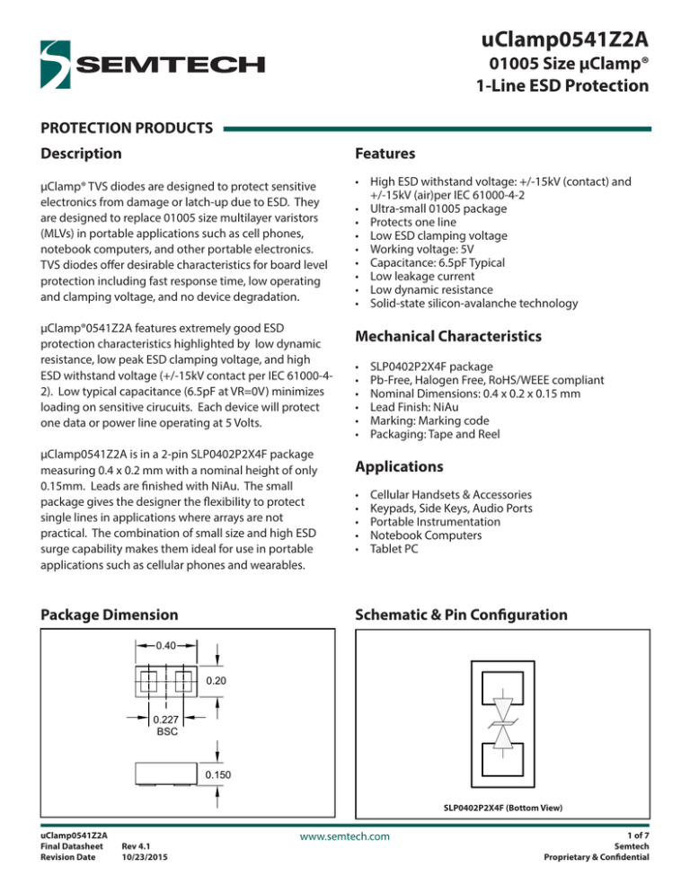
µClamp0541Z2A is in a 2-pin SLP0402P2X4F package
measuring 0.4 x 0.2 mm with a nominal height of only
0.15mm. Leads are finished with NiAu. The small
package gives the designer the flexibility to protect
single lines in applications where arrays are not
practical. The combination of small size and high ESD
surge capability makes them ideal for use in portable
applications such as cellular phones and wearables. Package Dimension
•
•
•
•
•
•
SLP0402P2X4F package
Pb-Free, Halogen Free, RoHS/WEEE compliant
Nominal Dimensions: 0.4 x 0.2 x 0.15 mm
Lead Finish: NiAu
Marking: Marking code
Packaging: Tape and Reel
Applications
•
•
•
•
•
Cellular Handsets & Accessories
Keypads, Side Keys, Audio Ports
Portable Instrumentation
Notebook Computers
Tablet PC
Schematic & Pin Configuration
0.40
0.20
0.227
BSC
0.150
SLP0402P2X4F (Bottom View)
uClamp0541Z2A
Final Datasheet
Revision Date
Rev 4.1
10/23/2015
www.semtech.com
1 of 7
Semtech
Proprietary & Confidential
Absolute Maximum Rating
Rating
Symbol
Value
Units
Peak Pulse Power (tp = 1.2/50µs)
PPK
30
W
Peak Pulse Current (tp = 1.2/50µs)
IPP
2
A
ESD per IEC 61000-4-2 (Air)
ESD per IEC 61000-4-2 (Contact)(1)
VESD
±15
±15
kV
Operating Temperature
TJ
-40 to +125
O
Storage Temperature
TSTG
-55 to +150
O
(1)
C
C
Electrical Characteristics (T=25OC unless otherwise specified)
Parameter
Symbol
Conditions
Reverse Stand-Off Voltage
VRWM
T = -40 to +125
Reverse Breakdown Voltage
VBR
It = 1mA
Reverse Leakage Current
IR
VRWM = 5V
Clamping Voltage
VC
ESD Clamping Voltage2
VC
Dynamic Resistance2,3
Junction Capacitance
Min.
6.5
Typ.
Max.
Units
5
V
8
9.5
V
5
25
nA
15
V
IPP = 2A, tp = 8/20µs
I= 4A, tlp = 0.2/100ns
11
I=16A, tlp = 0.2/100ns
18.5
RDYN
tlp = 0.2/100ns
0.62
CJ
VR = 0V, f = 1MHz
6.5
V
Ω
9
pF
Notes
1) Measured with a 20dB attenuator, 50 Ohm scope input impedance, 2GHz bandwidth. ESD gun return path connected to ESD ground plane. 2) Transmission Line Pulse Test (TLP) Settings: tp = 100ns, tr = 0.2ns, ITLP and V TLP averaging window: t1 = 70ns to t2 = 90ns.
3) Dynamic resistance calculated from ITLP = 4A to ITLP = 16A
uClamp0541Z2A
Final Datasheet
Revision Date
Rev 4.1
10/23/2015
www.semtech.com
2 of 7
Semtech
Proprietary & Confidential
Typical Characteristics
ESD Clamping (-8kV Contact per IEC 61000-4-2)
ESD Clamping (8kV Contact per IEC 61000-4-2)
35
30
0
25
-5
Clamping Voltage - VC (V)
Clamping Voltage - VC (V)
5
Measured with 50 Ohm scope input
impedance, 2GHz bandwidth. Corrected
for 50 Ohm, 20dB attenuator. ESD gun
return path connected to ESD ground plane.
20
15
10
5
-10
-15
-20
-25
-5
Measured with 50 Ohm scope input
impedance, 2GHz bandwidth. Corrected
for 50 Ohm, 20dB attenuator. ESD gun
return path connected to ESD ground plane.
-30
0
-10
0
10
20
30
40
50
60
70
-35
80
-10
0
10
20
30
40
Time (ns)
Time (ns)
-5
15
10
-10
-15
5
-20
0
-25
-5
0
5
10
15
20
25
30
-30
Transmission Line Pulse Test
(TLP) Settings:
tp = 100ns, tr = 0.2ns,
ITLP and VTLP averaging window:
t1 = 70ns to t2 = 90ns
-25
-20
-15
Clamping Voltage (V)
-5
0
Capacitance vs. Reverse Voltage
7
12
6
11
Junction Capacitance - CJ (pF)
Peak Clamping Voltage - VC (V)
-10
Clamping Voltage (V)
Clamping Characteristic (8/20us Waveform)
10
9
8
7
6
80
0
TLP Current (A)
TLP Current (A)
20
70
5
Transmission Line Pulse Test
(TLP) Settings:
tp = 100ns, tr = 0.2ns,
ITLP and VTLP averaging window:
t1 = 70ns to t2 = 90ns
25
60
TLP Characteristic (Negative Pulse)
TLP Characteristic (Positive Pulse)
30
50
TA = 25OC
Waveform: tp= 8x20us
0.5
uClamp0541Z2A
Final Datasheet
Revision Date
0.75
1
1.25
1.5
Peak Pulse Current - IPP (A)
Rev 4.1
10/23/2015
1.75
5
4
3
2
1
0
2
www.semtech.com
f = 1MHz
T=25oC
0
1
2
3
4
5
6
Voltage (V)
3 of 7
Semtech
Proprietary & Confidential
Application Information
Assembly Guidelines
The small size of this device means that some care must
be taken during the mounting process to insure reliablesolder joints. The figure at the right details Semtech’s
recommended mounting pattern. Recommended
assembly guidelines are shown in Table 1. Note that
these are only recommendations and should serve only
as a starting point for design since there are many factors
that affect the assembly process. Exact manufacturingparameters will require some experimentation to get
the desired solder application. Semtech’s recommendedmounting pattern is based on the following design
guidelines: Land Pattern
The recommended land pattern follows IPC standards
and is designed for maximum solder coverage. Detailed
dimensions are shown elsewhere in this document.
Solder Stencil
Stencil design is one of the key factors which will determine the volume of solder paste which is deposited onto
the land pad. The area ratio of the stencil aperture will
determine how well the stencil will print. The area ratio
takes into account the aperture shape, aperture size, and
stencil thickness. An area
ratio of 0.70 – 0.75 is preferred for the subject package.
The area ratio of a rectangular aperture is given as:
Recommended Mounting Pattern
Land Pattern
0.400
0.495
0.250
0.125
Component
0.185
0.200
Stencil Opening
All Dimensions are in mm.
Land Pad.
Stencil opening
Assembly Parameter
Laser cut, Electro-polished
Aperture shape
Rectangular with rounded
corners
Solder Stencil Thickness
Where:
L = Aperture Length
W = Aperture Width
T = Stencil Thickness
Solder Paste Type
uClamp0541Z2A
Final Datasheet
Revision Date
Rev 4.1
10/23/2015
Recommendation
Solder Stencil Design
Area Ratio = (L * W )/ (2 * (L + W) * T)
Solder Reflow Profile
Semtech recommends a stencil thickness of 0.100mm for
this device. The stencil should be laser cut with electropolishedfinish. The stencil should have a positive taper of
approximately 5 degrees. Electro polishing and tapering
the walls results in reduced surface friction and better
paste release. For small pitch components, Semtech
recommends a square aperture with rounded corners for
consistent solder release. Due to the small aperture size,
a solder paste with Type 4 or smaller particles are recommended.
Component
PCB Solder Pad Design
PCB Pad Finish
www.semtech.com
0.100 mm (0.004")
Type 4 size sphere or smaller
Per JEDEC J-STD-020
Non-Solder mask defined
OSP OR NiAu
4 of 7
Semtech
Proprietary & Confidential
Outline Drawing - SLP0402P2X4F
A
B
D
DIMENSIONS
MILLIMETERS
DIM
MIN NOM MAX
E
A
A1
b
D
E
e
L
N
aaa
bbb
TOP VIEW
A
SEATING
PLANE
aaa C
C
A1
D/2
bxN
bbb
0.125 0.150 0.175
0.000 0.010 0.050
0.115 0.135 0.150
0.370 0.400 0.430
0.170 0.200 0.230
0.227 BSC
0.088 0.108 0.123
2
0.08
0.10
C A B
E/2
LxN
e/2
e
BOTTOM VIEW
NOTES:
1. CONTROLLING DIMENSIONS ARE IN MILLIMETERS (ANGLES IN DEGREES).
Land Pattern - SLP0402P2X4F
DIMENSIONS
Z
G
Y
DIM
G
X
Y
Z
MILLIMETERS
0.125
0.200
0.160
0.445
X
NOTES:
1. CONTROLLING DIMENSIONS ARE IN MILLIMETERS (ANGLES IN DEGREES).
2. THIS LAND PATTERN IS FOR REFERENCE PURPOSES ONLY.
CONSULT YOUR MANUFACTURING GROUP TO ENSURE YOUR
COMPANY'S MANUFACTURING GUIDELINES ARE MET.
uClamp0541Z2A
Final Datasheet
Revision Date
Rev 4.1
10/23/2015
www.semtech.com
5 of 7
Semtech
Proprietary & Confidential
Marking Code
Tape and Reel Specification
Ordering Information
Part Number
Qty per Reel
Reel Size
uClamp0541Z2ATKT
20,000
7”
MicroClamp, uClamp and µClamp are registered trademarks of Semtech
Corporation.
uClamp0541Z2A
Final Datasheet
Revision Date
Rev 4.1
10/23/2015
www.semtech.com
6 of 7
Semtech
Proprietary & Confidential
IMPORTANT NOTICE
Information relating to this product and the application or design described herein is believed to be reliable, however such information is provided as a
guide only and Semtech assumes no liability for any errors in this document, or for the application or design described herein. Semtech reserves the right
to make changes to the product or this document at any time without notice. Buyers should obtain the latest relevant information before placing orders
and should verify that such information is current and complete. Semtech warrants performance of its products to the specifications applicable at the time
of sale, and all sales are made in accordance with Semtech’s standard terms and conditions of sale.
SEMTECH PRODUCTS ARE NOT DESIGNED, INTENDED, AUTHORIZED OR WARRANTED TO BE SUITABLE FOR USE IN LIFE-SUPPORT APPLICATIONS, DEVICES
OR SYSTEMS, OR IN NUCLEAR APPLICATIONS IN WHICH THE FAILURE COULD BE REASONABLY EXPECTED TO RESULT IN PERSONAL INJURY, LOSS OF LIFE
OR SEVERE PROPERTY OR ENVIRONMENTAL DAMAGE. INCLUSION OF SEMTECH PRODUCTS IN SUCH APPLICATIONS IS UNDERSTOOD TO BE UNDERTAKEN
SOLELY AT THE CUSTOMER’S OWN RISK. Should a customer purchase or use Semtech products for any such unauthorized application, the customer shall
indemnify and hold Semtech and its officers, employees, subsidiaries, affiliates, and distributors harmless against all claims, costs damages and attorney
fees which could arise.
The Semtech name and logo are registered trademarks of the Semtech Corporation. All other trademarks and trade names mentioned may be marks and
names of Semtech or their respective companies. Semtech reserves the right to make changes to, or discontinue any products described in this document
without further notice. Semtech makes no warranty, representation or guarantee, express or implied, regarding the suitability of its products for any
particular purpose. All rights reserved.
© Semtech 2015
Contact Information
Semtech Corporation
200 Flynn Road, Camarillo, CA 93012
Phone: (805) 498-2111, Fax: (805) 498-3804
www.semtech.com
uClamp0541Z2A
Final Datasheet
Revision Date
4.1
10/23/2015
7 of 7
Semtech
Proprietary & Confidential
