SC4525C/D Application Note
Converting SC4525A/B to SC4525C/D
AN-PM-1104
POWER MANAGEMENT
This application note is intended to assist designers in the
transition from Semtech’s SC4525A and SC4525B step-down
switching regulators to the SC4525C and SC4525D devices.
The SC4525C and SC4525D regulators share the identical
footprint as the “A” and “B” versions, so existing customers
will not need to make any PCB changes. Only minor external component value adjustments are necessary to ensure
the SC4525C and SC4525D perform identically to the
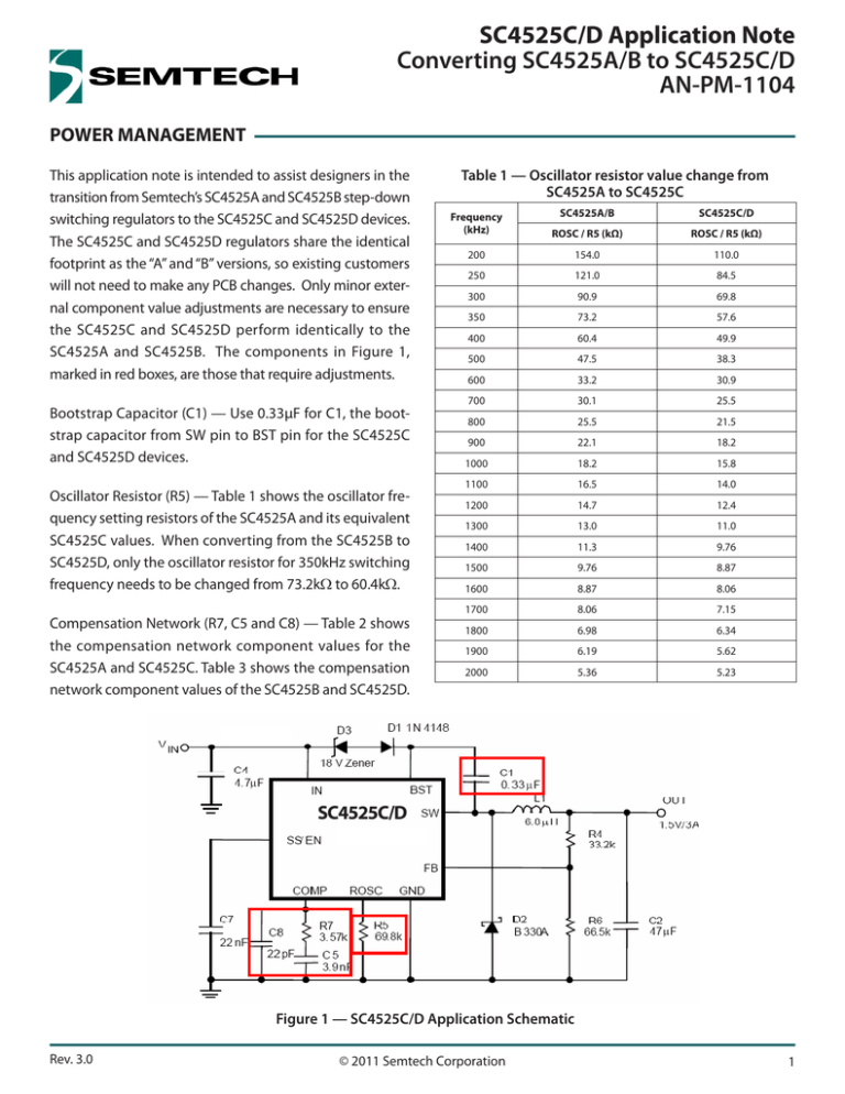
SC4525A and SC4525B. The components in Figure 1,
marked in red boxes, are those that require adjustments.
Bootstrap Capacitor (C1) — Use 0.33μF for C1, the bootstrap capacitor from SW pin to BST pin for the SC4525C
and SC4525D devices.
Oscillator Resistor (R5) — Table 1 shows the oscillator frequency setting resistors of the SC4525A and its equivalent
SC4525C values. When converting from the SC4525B to
SC4525D, only the oscillator resistor for 350kHz switching
frequency needs to be changed from 73.2kW to 60.4kW.
Compensation Network (R7, C5 and C8) — Table 2 shows
the compensation network component values for the
SC4525A and SC4525C. Table 3 shows the compensation
network component values of the SC4525B and SC4525D.
Table 1 — Oscillator resistor value change from
SC4525A to SC4525C
Frequency
(kHz)
SC4525A/B
SC4525C/D
ROSC / R5 (kΩ)
ROSC / R5 (kΩ)
200
154.0
110.0
250
121.0
84.5
300
90.9
69.8
350
73.2
57.6
400
60.4
49.9
500
47.5
38.3
600
33.2
30.9
700
30.1
25.5
800
25.5
21.5
900
22.1
18.2
1000
18.2
15.8
1100
16.5
14.0
1200
14.7
12.4
1300
13.0
11.0
1400
11.3
9.76
1500
9.76
8.87
1600
8.87
8.06
1700
8.06
7.15
1800
6.98
6.34
1900
6.19
5.62
2000
5.36
5.23
SC4525C/D
Figure 1 — SC4525C/D Application Schematic
Rev. 3.0
© 2011 Semtech Corporation
SC4525C/D Application Note
Table 2 — Compensation component value change from SC4525A to SC4525C
SC4525A
Recommended Parameters
Typical Applications
VIN (V)
VO (V)
IO (A)
1.5
2.5
3.3
12
3
5
7.5
10
1.5
3.3
3
5
L1 (μH)
R7 (kΩ)
C5 (nF)
L1 (μH)
R7 (kΩ)
C5 (nF)
500
3.3
10
2.2
3.3
5.23
3.9
500
4.7
16.2
2.2
4.7
8.45
3.9
1000
2.2
29.4
0.47
2.2
15.4
0.82
500
6.8
23.2
2.2
6.8
12.1
3.9
1000
3.3
39.2
0.47
3.3
20.5
0.82
500
6.8
29.4
2.2
6.8
15.4
3.9
1000
3.3
69.8
0.47
3.3
36.5
0.82
7.5
10
C2 (μF)
C8 (pF)
500
6.8
43.2
2.2
6.8
22.6
3.9
1000
3.3
90.9
0.47
3.3
47.5
0.82
500
3.3
69.8
2.2
3.3
36.5
3.9
1000
2.2
133
0.47
6.8
6.81
2.2
300
2.5
24
FSW (Hz)
SC4525C
Recommended Parameters
47
Not Recommended
10
6.8
6.8
3.57
3.9
6.49
3.9
500
6.8
12.4
2.2
1000
2.2
29.4
0.47
500
6.8
23.2
2.2
6.8
12.1
3.9
1000
3.3
43.2
0.47
3.3
22.6
0.82
500
8.2
29.4
2.2
8.2
15.4
3.9
1000
4.7
59
0.47
4.7
30.9
0.82
C8 (pF)
no
22
Not Recommended
500
10
49.9
2.2
10
26.1
3.9
1000
4.7
100
0.47
4.7
52.3
0.82
500
15
59
2.2
15
30.9
3.9
1000
6.8
133
0.47
6.8
69.8
0.82
Snubber
1Ω+
220pF
no
Table 3 — Compensation component value change from SC4525B to SC4525D
SC4525B
Recommended Parameters
Typical Applications
VIN (V)
VO (V)
3.3
5
L1 (μH)
R7 (kΩ)
C5 (nF)
1.0
3.3
7.15
3.2
2.0
2.2
12.4
1.5
1.5
3.3
7.15
3.3
2.5
4.7
12.4
2.2
4.7
14.32
1.5
4.7
7.15
3.2
2.5
6.8
13.3
2.2
3.3
8.2
16.5
1.5
5
10
22.1
1.0
7.5
10
34.8
1.0
3.3
1.5
12
AN-PM-1104
IO (A)
3
C2 (μF)
47
SC4525D
Recommended Parameters
C8 (pF)
22
33
47
33
22
L1 (μH)
R7 (kΩ)
C5 (nF)
3.3
3.74
6.8
2.2
6.49
3.3
3.3
3.74
6.8
4.7
6.49
4.7
4.7
7.5
3.3
4.7
3.74
6.8
6.8
6.98
4.7
8.2
8.66
3.3
10
11.5
2.2
10
18.2
2.2
C8 (pF)
47
68
82
68
47
SC4525C/D Application Note
VOUT > 8V Applications
If VOUT > 8V then use a small Schottky diode D1 (BAT54 or similar) for bootstrapping.
D1
BST
VIN
C1
SC4525C/D
VO > 8V
SW
IN
GND
D2
Figure 2 — Bootstrapping the SC4525C/D when VOUT > 8V
AN-PM-1104
SC4525C/D Application Note
Electrical Characteristics Changes
Some electrical specifications have changed on the SC4525C and SC4525D. The differences between the SC4525A/B and
SC4525C/D are minor and have minimal impact on the circuit performance. The comparison results are shown in Tables
4 and 5.
Table 4 — SC4525A and SC4525C Electrical Characteristic Comparison
Parameter
SC4525A
Minimum
Typical
VIN Quiescent Current in Shutdown (μA)
SC4525C
Maximum
Minimum
Typical
50
Maximum
52
Error Amplifier Transconductance (μΩ-1)
280
300
COMP Pin to Switch Current Gain (A/V)
12
15.2
Foldback Frequency (kHz) — ROSC = 93.1kΩ(1)
240
300
360
230
Foldback Frequency (kHz) — ROSC = 12.1kΩ, VFB = 0
110
230
350
100
Foldback Frequency (kHz) — ROSC = 93.1kΩ(1), VFB = 0
50
110
170
35
60
90
SS/EN Switching Threshold (V)
1
1.13
1.3
0.95
1.2
1.4
Soft-start Charging Current (μA) — VSS/EN = 0V
Soft-start Charging Current (μA) — VSS/EN = 1.5V
300
250
1.7
1.2
2
370
1.9
2.8
1.6
2.4
Integrated Current Sense Resistor (mΩ)
4.1
3.53
Internal Current Limit Voltage Threshold (mV)
20
18
3.2
NOTE: (1) 73.2kΩ for the SC4525C
Table 5 — SC4525B and SC4525D Electrical Characteristic Comparison
Parameter
SC4525B
Minimum
Typical
VIN Quiescent Current in Shutdown (μA)
SC4525D
Maximum
Minimum
Typical
50
52
Error Amplifier Transconductance (μΩ-1)
280
300
COMP Pin to Switch Current Gain (A/V)
12
15.2
Foldback Frequency (kHz) — ROSC = 73.2kΩ(1), VFB = 0
SS/EN Switching Threshold (V)
35
100
185
35
65
100
0.95
1.13
1.35
0.95
1.2
1.4
Soft-start Charging Current (μA) — VSS/EN = 0V
Soft-start Charging Current (μA) — VSS/EN = 1.5V
Maximum
1.7
1.2
2
1.9
2.8
1.6
2.4
3.2
NOTE: (1) 60.4kΩ for the SC4525D
AN-PM-1104
SC4525C/D Application Note
© Semtech 2011
All rights reserved. Reproduction in whole or in part is prohibited without the prior written consent of the copyright
owner. The information presented in this document does not form part of any quotation or contract, is believed to be
accurate and reliable and may be changed without notice. No liability will be accepted by the publisher for any consequence of its use. Publication thereof does not convey nor imply any license under patent or other industrial or intellectual property rights. Semtech assumes no responsibility or liability whatsoever for any failure or unexpected operation
resulting from misuse, neglect improper installation, repair or improper handling or unusual physical or electrical stress
including, but not limited to, exposure to parameters beyond the specified maximum ratings or operation outside the
specified range.
SEMTECH PRODUCTS ARE NOT DESIGNED, INTENDED, AUTHORIZED OR WARRANTED TO BE SUITABLE FOR USE IN LIFESUPPORT APPLICATIONS, DEVICES OR SYSTEMS OR OTHER CRITICAL APPLICATIONS. INCLUSION OF SEMTECH PRODUCTS
IN SUCH APPLICATIONS IS UNDERSTOOD TO BE UNDERTAKEN SOLELY AT THE CUSTOMER’S OWN RISK. Should a customer
purchase or use Semtech products for any such unauthorized application, the customer shall indemnify and hold
Semtech and its officers, employees, subsidiaries, affiliates, and distributors harmless against all claims, costs damages
and attorney fees which could arise.
Notice: All referenced brands, product names, service names and trademarks are the property of their respective
owners.
Contact Information
Semtech Corporation
Power Management Products Division
200 Flynn Road, Camarillo, CA 93012
Phone: (805) 498-2111 Fax: (805) 498-3804
www.semtech.com
AN-PM-1104


