SX1710
DATASHEET
WIRELESS SENSING & TIMING
Broadband High Efficiency RF Power Amplifier
100 MHz to 1 GHz
GENERAL DESCRIPTION
KEY PRODUCT FEATURES
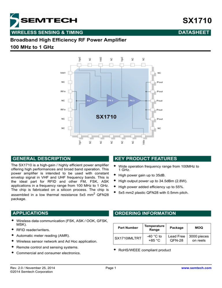
The SX1710 is a high-gain / highly efficient power amplifier
offering high performances and broad band operation. This
power amplifier is intended to be used with constant
envelop signal in VHF and UHF frequency bands. This is
the ideal part for RFID and other FM, FSK, ASK
applications in a frequency range from 100 MHz to 1 GHz.
The chip is fabricated on a silicon process. The chip is
assembled in a low thermal resistance 5x5 mm2 QFN28
package.
APPLICATIONS
Wireless data communication (FSK, ASK / OOK, GFSK,
MSK).
RFID reader/writers.
Wireless sensor network and Ad Hoc application.
Remote control and sensing systems.
Commercial and consumer electronics.
Rev. 2.0 / November 25, 2014
©2014 Semtech Corporation
Wide operation frequency range from 100MHz to
1 GHz.
High power gain up to 35dB.
High output power up to 34.5dBm (2.8W).
High power added efficiency up to 55%.
5x5 mm2 plastic QFN28 with 0.5mm pitch.
ORDERING INFORMATION
Automatic meter reading (AMR).
Part Number
Temperature
Range
Package
MOQ
SX1710IMLTRT
-40 °C to
+85 °C
Lead Free
QFN-28
3000 pieces
on reels
Page 1
RoHS/WEEE compliant product
www.semtech.com
SX1710
DATASHEET
WIRELESS SENSING & TIMING
Table of contents
Section
1.
2.
3.
4.
5.
Page
General Description ................................................................................................................................................. 3
1.1. Package Marking ............................................................................................................................................. 3
1.2. Pin Description .................................................................................................................................................4
Electrical Characteristics ......................................................................................................................................... 5
2.1.
ESD Notice ...................................................................................................................................................... 5
2.2.
Absolute Maximum Ratings ............................................................................................................................. 5
2.3.
Operating Range.............................................................................................................................................. 5
2.4. Specifications ...................................................................................................................................................6
Application Information ............................................................................................................................................ 7
3.1.
General Application Schematic........................................................................................................................ 7
3.2. General Application Layout ..............................................................................................................................8
Packaging Information ............................................................................................................................................. 9
Revision History..................................................................................................................................................... 11
FIGURES
Figure 1
Package Marking .................................................................................................................................3
Figure 2
SX1710 test and application circuit for 450MHz Applications ..............................................................7
Figure 3
SX1710 Test and Application Layout for VHF and UHF Operations (59.18mm by 33mm) ..................8
Figure 4
Description of the SX1710 Package .....................................................................................................9
Figure 5
Land Pattern .......................................................................................................................................10
TABLES
Table 1
Pin Description .....................................................................................................................................4
Table 2
Absolute Maximum Ratings ..................................................................................................................5
Table 3
Operating Range ..................................................................................................................................5
Table 4
Specifications .......................................................................................................................................6
Table 5
Revision History ..................................................................................................................................11
Rev. 2.0 / November 25, 2014
©2014 Semtech Corporation
Page 2
www.semtech.com
SX1710
DATASHEET
WIRELESS SENSING & TIMING
1. General Description
SX1710 is a three-stage wide-band power amplifier device with high gain. An input power of -5 dBm is required to achieve
its fully saturate output power.
In normal application for signal with constant envelope, the first and second stages of the amplifier operate in class-A and
class-AB mode, respectively. The third stage of the amplifier operates in class-C mode. Its DC current will be increased
with RF input signal.
1.1. Package Marking
Figure 1. Package Marking
Note:
yyww:
Date Code
xxxxx:
Lot No.
Rev. 2.0 / November 25, 2014
©2014 Semtech Corporation
Page 3
www.semtech.com
SX1710
DATASHEET
WIRELESS SENSING & TIMING
1.2. Pin Description
The description of the pins of the circuit is given in Table 1 below.
Table 1
Pin Description
Number
Name
Type
Description
1
Vdd1
Power Supply
Power Supply for first stage
2
NC
Floating
No Connection
3
RFin
RF Input
RF Input and off chip DC blocking capacitor required
4
NC
Floating
No Connection
5
RFin
RF Input
Same as Pin 3
6
NC
7
NC
Floating
No Connection
8
Vgs1
Analog Input
Bias Input for first stage
9
GND
10
GND
Ground
Ground
11
NC
12
NC
Floating
No Connection
13
NC
14
Vdda
Power Supply
Power Supply for ESD
15
NC
16
RFout
17
RFout
18
RFout
19
RFout
20
RFout
21
NC
22
NC
23
NC
24
No Connection
RF Output
Power Supply and RF Output for the output stage
Floating
No Connection
Vgs3
Analog Input
Bias Input for Output Stage
25
NC
Floating
No Connection
26
Vdd2
Power Supply
Power Supply for Second Stage
27
NC
Floating
No Connection
28
Vgs2
Analog Input
Bias Input for Second Stage
Snug
GND
Ground
Ground and Thermal Dissipation
Rev. 2.0 / November 25, 2014
©2014 Semtech Corporation
Page 4
www.semtech.com
SX1710
DATASHEET
WIRELESS SENSING & TIMING
2. Electrical Characteristics
2.1. ESD Notice
The SX1710 is an RF Power Amplifier device which satisfies the ff:
Class 1A of the JEDEC standard JESD22-A114 (Human Body Model) on all pins
Class I of the JEDEC standard JESD22-C101 (Charge Device Model) on all pins
CAUTION: ESD sensitive device!
It should thus be handled with all the necessary ESD precautions to avoid any permanent damage!
2.2. Absolute Maximum Ratings
Stresses above the values listed below may cause permanent device failure. Exposure to absolute maximum ratings for
extended periods may affect device reliability.
Table 2
Absolute Maximum Ratings
Symbol
Description
Min.
Max.
Unit
-0.5
5.0
V
-
2.2
A
-0.5
2.0
V
Vdsmr
Drain to source voltage (transient)
Idsmr
Total supply current
Vgsmr
Gate to source voltage
Ovswrmr
Output load VSWR
-
10:1
-
Irfmr
Input level
-
15
dBm
Tsoldmr
Soldering temperature (lead)
-
260
°C
Tmr
Storage temperature
-40
125
°C
Min.
Max.
Unit
2.3. Operating Range
Conditions: VDD must be powered up before or in parallel with VGG (Vbias)
Table 3
Operating Range
Symbol
Description
VDD
Supply Voltage
2.5
5.0
V
VGG (Vbias)
Bias Main Supply
2.5
4.0
V
VGS
Bias Control Voltage per stage
0.7
1.7
V
Tja
Thermal Resistance: junction-to-ambient
30.21
-
°C/W
Trop
Temperature
-40
85
°C
Rev. 2.0 / November 25, 2014
©2014 Semtech Corporation
Page 5
www.semtech.com
SX1710
DATASHEET
WIRELESS SENSING & TIMING
2.4. Specifications
Nominal conditions: Measurements performed on the basis of the general application circuitry.
Temp = 25 °C, VDD = 4.0V, Vbias= 3.3V, RF frequency = 465 MHz, Pin = 0 dBm CW, unless otherwise specified.
Table 4
Specifications
Description
Conditions
Min.
Typ.
Max.
Unit
100
-
1000
MHz
Frequency Range
Nominal
Supply Current
VDD = 4.0 V, Pout = 33 dBm
-
1.23
-
A
Maximum Output Power (Pmax)
Nominal
-
33
-
dBm
Power Added Efficiency
VDD = 4.0 V, Pout = 33 dBm
-
41
-
%
Input Power for Pmax
Nominal
-
0
-
dBm
Reverse Isolation
Nominal
-
-60
-
dB
Second Harmonic Level
Nominal
-
-42
-
dBc
Third Harmonic Level
Nominal
-
-50
-
dBc
Fourth Harmonic Level
Nominal
-
-33
-
dBc
Input Return Loss
Externally connected to 50Ω
-
6.2:1
-
-
Output Return Loss
Externally connected to 50Ω
-
10:1
-
-
Rev. 2.0 / November 25, 2014
©2014 Semtech Corporation
Page 6
www.semtech.com
SX1710
DATASHEET
WIRELESS SENSING & TIMING
3. Application Information
3.1. General Application Schematic
The typical test and application schematics including harmonics filtering for 450MHz operation is shown in Figure 2.
Figure 2. SX1710 test and application circuit for 450MHz Applications
Rev. 2.0 / November 25, 2014
©2014 Semtech Corporation
Page 7
www.semtech.com
SX1710
DATASHEET
WIRELESS SENSING & TIMING
3.2. General Application Layout
The typical test and application layout including harmonics filtering for VHF and UHF operation is shown in figure 3
Figure 3. SX1710 Test and Application Layout for VHF and UHF Operations (59.18mm by 33mm)
A special care must be taken care for the multi via layout of the PCB. 10 mil hole size is recommended and via must be
trough top layer to bottom layer. If transmit duty cycle is high, a good thermal dissipation is necessary and a heat sink must
be required.
Please contact Semtech support, specific reference designs are available to fit your application.
Rev. 2.0 / November 25, 2014
©2014 Semtech Corporation
Page 8
www.semtech.com
SX1710
DATASHEET
WIRELESS SENSING & TIMING
4. Packaging Information
SX1710 is available in a 28-lead QFN package as shown in Figure 4 below.
Figure 4. Description of the SX1710 Package
Rev. 2.0 / November 25, 2014
©2014 Semtech Corporation
Page 9
www.semtech.com
SX1710
DATASHEET
WIRELESS SENSING & TIMING
Figure 5. Land Pattern
Rev. 2.0 / November 25, 2014
©2014 Semtech Corporation
Page 10
www.semtech.com
SX1710
DATASHEET
WIRELESS SENSING & TIMING
5. Revision History
Table 5
Revision
1
2
Revision History
Date
May 2013
November 2014
Rev. 2.0 / November 25, 2014
©2014 Semtech Corporation
Comment
Preliminary Datasheet
Specification and Application board changes
Page 11
www.semtech.com
SX1710
DATASHEET
WIRELESS SENSING & TIMING
© Semtech 2014
All rights reserved. Reproduction in whole or in part is prohibited without the prior written consent of the copyright owner. The
information presented in this document does not form part of any quotation or contract, is believed to be accurate and reliable
and may be changed without notice. No liability will be accepted by the publisher for any consequence of its use. Publication
thereof does not convey nor imply any license under patent or other industrial or intellectual property rights. Semtech assumes
no responsibility or liability whatsoever for any failure or unexpected operation resulting from misuse, neglect improper
installation, repair or improper handling or unusual physical or electrical stress including, but not limited to, exposure to
parameters beyond the specified maximum ratings or operation outside the specified range.
SEMTECH PRODUCTS ARE NOT DESIGNED, INTENDED, AUTHORIZED OR WARRANTED TO BE SUITABLE FOR USE IN
LIFE-SUPPORT APPLICATIONS, DEVICES OR SYSTEMS OR OTHER CRITICAL APPLICATIONS. INCLUSION OF
SEMTECH PRODUCTS IN SUCH APPLICATIONS IS UNDERSTOOD TO BE UNDERTAKEN SOLELY AT THE CUSTOMER’S
OWN RISK. Should a customer purchase or use Semtech products for any such unauthorized application, the customer shall
indemnify and hold Semtech and its officers, employees, subsidiaries, affiliates, and distributors harmless against all claims,
costs damages and attorney fees which could arise.
Contact information
Semtech Corporation
Wireless & Sensing Products Division
200 Flynn Road, Camarillo, CA 93012
Phone: (805) 498-2111 Fax: (805) 498-3804
E-mail: sales@semtech.com
support_rf@semtech.com
Internet: http://www.semtech.com
Rev. 2.0 / November 25, 2014
©2014 Semtech Corporation
Page 12
www.semtech.com


