MP6510
4.5V-to-16V,1.2A, Single-Phase
Brushless DC Motor Driver
The Future of Analog IC Technology
FEATURES
DESCRIPTION
The MP6510 is a single-phase, brushless, DC
motor driver with integrated power MOSFETs. It
drives single-phase brushless DC motors. The
input voltage ranges from 4.5V to 16V, with a
maximum output current of 1.2A at room
temperature.
The MP6510 controls the rotational speed either
through the input voltage or the PWM signal.
Other features include selectable minimum
rotational speed, a rotational-speed indicator,
built-in input over-voltage protection, built-in
locked-rotor
protection,
locked-rotor
state
indicator, thermal shutdown, and 1.2V integrated
Hall bias voltage.
The MP6510 is available in 5.0mm×6.4mm
TSSOP16 and 3mm×3mm QFN16 package.
• 4.5V-to-16V Operating Voltage
• Integrated Power MOSFETs (HS: 370mΩ; LS:
230mΩ)
• Maximum Output Current 1.2A
• Low Quiescent Current (Not including Hall
Sensor) of 1.4mA
• Speed Control via Input Voltage or PWM Signal
• Programmable Minimum Speed
• Rotational Speed Indicator
• Locked-Rotor Indicator
• Locked-Rotor Protection and Automatic
Recovery
• Thermal Protection and Automatic Recovery
• Built-in Input OVP and Automatic Recovery
• Hall Bias Voltage(1.2V) Integrated;
• Available in TSSOP16 (5.0×6.4mm) and QFN16
(3×3mm) Package
APPLICATIONS
• CPU Fan for Personal Computers or Servers
•Brushless DC Motor Driver
All MPS parts are lead-free and adhere to the RoHS directive. For MPS green
status, please visit MPS website under Quality Assurance.
“MPS” and “The Future of Analog IC Technology” are Registered Trademarks of
Monolithic Power Systems, Inc.
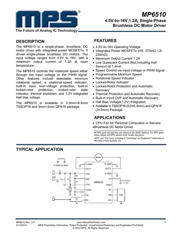
TYPICAL APPLICATION
Motor
VIN
GND
D1
R1
CIN
P-GND
P-GND
P-GND S-GND
OUT1
OUT2
VCC
S-GND
CT
RMI
R3
R2
VTH
R4
CP=100pF
VIN
R5
MP6510
CT=0.47µF
to 1µF
VREF
COSC
IN-
FG
HB
RD
IN+
Hall
R6
MP6510 Rev.1.01
4/14/2014
www.MonolithicPower.com
MPS Proprietary Information. Patent Protected. Unauthorized Photocopy and Duplication Prohibited.
© 2014 MPS. All Rights Reserved.
1
MP6510—4.5V-TO-16V, 1.2A, SINGLE-PHASE, BRUSHLESS DC MOTOR DRIVER
ORDERING INFORMATION
Part Number
MP6510DM-LF*
MP6510DQ-LF**
Package
TSSOP16 (5.0×6.4mm)
QFN16 (3×3mm)
Top Marking
MP6510
XXXX
* For Tape & Reel, add suffix –Z (eg. MP6510DM–Z);
For RoHS compliant packaging, add suffix –LF (e.g. MP6510DM–LF–Z)
** For Tape & Reel, add suffix –Z (eg. MP6510DQ–Z);
For RoHS compliant packaging, add suffix –LF (e.g. MP6510DQ–LF–Z)
PACKAGE REFERENCE
TOP VIEW
PIN 1 ID
P-GND
P-GND
1
16
OUT1
2
15
OUT2
VCC
3
14
S-GND
RMI
1
12 OUT2
RMI
4
13
CT
VTH
2
11 SGND
VTH
5
12
VREF
COSC
3
COSC
6
11
IN-
FG
4
FG
7
10
HB
RD
8
9
IN+
MP6510
TSSOP16
VCC .................................................... 0V to 20V
OUT1, OUT2 .................................... -1V to 20V
FG, RD .......................................... -0.3V to 18V
All Other Pins ................................ -0.3V to 6.5V
Continuous Power Dissipation…(TA = +25°C) (2)
……………………………………………....1.17W
Junction Temperature .............................. 150°C
Storage Temperature .............. –55°C to +150°C
(3)
VCC ................................................. 4.5V to 16V
VTH ..................................................... 0V to 6V
IN+, IN- ............................................. 0.2V to 3V
Operating Junction Temp. (TJ). -40°C to +125°C
MP6510 Rev.1.01
4/14/2014
16
15
14
13
MP6510
10
CT
9 VREF
5
6
7
RD
IN+
HB
EXPOSED PAD ON BACKSIDE
NOT CONNECTED
8
IN-
QFN16
ABSOLUTE MAXIMUM RATINGS (1)
Recommended Operating Conditions
OUT1 PGND VCC PGND
Thermal Resistance
(4)
θJA
θJC
TSSOP16 (5.0×6.4mm) .......... 90 ...... 30 ... °C/W
QFN16 (3×3mm)..................... 60 ...... 12 ... °C/W
Notes:
Exceeding these ratings may damage the device.
The maximum allowable power dissipation is a function of the
maximum junction temperature TJ (MAX), the junction-toambient thermal resistance θJA, and the ambient temperature
TA. The maximum allowable continuous power dissipation at
any ambient temperature is calculated by PD (MAX) = (TJ
(MAX)-TA)/θJA. Exceeding the maximum allowable power
dissipation will cause excessive die temperature, and the
regulator will go into thermal shutdown. Internal thermal
shutdown circuitry protects the device from permanent
damage.
The device is not guaranteed to function outside of its operating
conditions.
Measured on JESD51-7, 4-layer PCB.
www.MonolithicPower.com
MPS Proprietary Information. Patent Protected. Unauthorized Photocopy and Duplication Prohibited.
© 2014 MPS. All Rights Reserved.
2
MP6510—4.5V-TO-16V, 1.2A, SINGLE-PHASE, BRUSHLESS DC MOTOR DRIVER
ELECTRICAL CHARACTERICS
TA=25°C, VCC=12V, unless otherwise noted.
Parameter
Circuit Current at Locked-Rotor
Protection Mode
Reference Voltage
HB Voltage
COSC High-Level Voltage
COSC Low-Level Voltage
COSC Oscillator Frequency
CT Pin High-level Voltage
CT Pin Low-level Voltage
ICT Charge Current
ICT Discharge Current
ICT Charge/Discharge Ratio
High-Side Switch-On Resistance
Low-Side Switch-On Resistance
Current Limit Gain
Current Limit
ICC
VREF
VHB
VCOSC_H
VCOSC_L
fCOSC
VCTH
VCTL
ICT1
ICT2
rCT
RDS1
RDS2
GC
IPEAK
Under-Voltage–Lockout Threshold—
Rising
Under-Voltage–Lockout Threshold—
Hysteresis
RD/FG Output Pin Low-level Voltage
RD/FG Output Pin Leakage Current
OVP Threshold Rising
OVP Threshold Hysteresis
MP6510 Rev.1.01
4/14/2014
Symbol
Condition
Min
Typ
Max
Unit
VCC=20V
1.0
1.4
2
mA
IVREF=5mA
IHB=5mA
5.6
1.1
3.45
1.8
26.4
3.4
1.63
1.1
0.08
7
6.2
1.2
3.75
2.1
35.6
3.86
1.83
2.85
0.25
18
420
V
V
V
V
kHz
V
V
μA
μA
VCC=12V TA=25°C
5.9
1.15
3.6
1.95
31
3.63
1.73
1.95
0.16
12
370
VCC=12V TA=25°C
230
260
mΩ
CP=100pF
9
A/V
IN+ - IN- =±50mV
0.4
0.7
1.3
IN+ - IN- =±100mV
0.8
1
1.8
IN+ - IN- =±150mV
1
1.4
2.3
3.57
3.75
3.93
190
VRDL/FGL
VRDL/FGL
IRD/FG=5mA
VRD/FG=12V
19
0.1
20
1.7
www.MonolithicPower.com
MPS Proprietary Information. Patent Protected. Unauthorized Photocopy and Duplication Prohibited.
© 2014 MPS. All Rights Reserved.
mΩ
A
V
mV
0.35
1
21
V
μA
V
V
3
MP6510—4.5V-TO-16V, 1.2A, SINGLE-PHASE, BRUSHLESS DC MOTOR DRIVER
PIN FUNCTIONS
Pin #
(TSSOP16)
Pin #
(QFN16)
Name
Description
1,16
2
3
4
5
13,15
16
14
1
2
P-GND
OUT1
VCC
RMI
VTH
6
3
COSC
7
4
FG
8
5
RD
9
10
6
7
IN+
HB
Power Ground.
Motor Driver Output 1.
Power Supply.
Minimum Rotational Speed Set.
Rotational Speed Control. Use DC voltage or PWM signal.
Oscillator Setting. Connect this pin to an external capacitor to set the
switch frequency.
Rotational Speed Detector. Connect to an external power source through
a pull-up resistor.
Locked-Rotor Protection Detector. Connect to an external power source
through a pull-up resistor.
Hall Sensor Input+. For rotor position detection and current limit setting.
Hall Sensor Bias Regulator Output. Powers the external Hall sensor.
11
12
8
9
INVREF
13
10
CT
14
15
11
12
Exposed
Pad
S-GND
OUT2
MP6510 Rev.1.01
4/14/2014
NC
Hall Sensor Input-. For rotor position detection and current limit setting.
Reference Voltage Output.
Locked-Rotor Protection and Recovery Time Set. Connect to an external
capacitor to set the recovery time.
Ground for Control Circuit.
Motor Driver Output 2.
Not Connected. Connect exposed thermal pad to power ground for better
thermal performance.
www.MonolithicPower.com
MPS Proprietary Information. Patent Protected. Unauthorized Photocopy and Duplication Prohibited.
© 2014 MPS. All Rights Reserved.
4
MP6510—4.5V-TO-16V, 1.2A, SINGLE-PHASE, BRUSHLESS DC MOTOR DRIVER
TYPICAL CHARACTERISTICS
VIN=12V, fCOSC=30kHz
UVLO vs. Temperature
ICC vs. Temperature
3.75
VCC Breakdown Voltage vs.
Temperature
1.60
26.0
25.5
1.55
3.72
3.71
25.0
VCC BV (V)
3.73
ICC (mA)
UVLO (V)
3.74
1.50
24.5
24.0
23.5
1.45
23.0
1.40
-40 -20 0
22.0
-40 -20
22.5
3.70
-40 -20 0 20 40 60 80 100 120 140
VHB vs. Temperature
1.17
6.000
1.166
5.975
1.162
5.950
1.158
31.0
VHB (V)
FREQUENCY (kHz)
31.5
30.5
30.0
1.154
1.150
1.146
1.142
0 20 40 60 80 100120140
MP6510 Rev.1.01
4/14/2014
1.13
-40 -20 0
5.900
5.875
5.825
1.134
29.0
-40 -20
5.925
5.850
1.138
29.5
0 20 40 60 80 100120 140
VREF vs. Temperature
VREF (V)
32.0
Frequency vs.
Temperature
20 40 60 80 100 120140
20 40 60 80 100 120140
5.800
-40 -20 0 20 40 60 80 100 120 140
www.MonolithicPower.com
MPS Proprietary Information. Patent Protected. Unauthorized Photocopy and Duplication Prohibited.
© 2014 MPS. All Rights Reserved.
5
MP6510—4.5V-TO-16V, 1.2A, SINGLE-PHASE, BRUSHLESS DC MOTOR DRIVER
TYPICAL PERFORMANCE CHARACTERISTICS
fCOSC=30kHz, CT=1μF, VTH=0V, VIN=12V, CIN=10μF, Lmotor=5mH, Rmotor=10Ω, TA=25ºC, unless
otherwise noted.
Current Limit vs.
Delta Hall Voltage
Steady State
Locked-rotor Protection
2 Duty=50%
CURRENT LIMIT(A)
1.8
1.6
VOUT1
10V/div.
VOUT2
10V/div.
VOUT1
10V/div.
1.4
1.2
VOUT2
10V/div.
1
VRD
5V/div.
0.8
0.6
VFG
5V/div.
IOUT
1A/div.
0.4
0.2
0
0
50
100
150 200
250 300
Power Ramp Up
Power Ramp Down
VOUT1
10V/div.
VOUT1
10V/div.
VOUT2
10V/div.
VOUT2
10V/div.
VIN
10V/div.
VIN
10V/div.
IOUT
1A/div.
IOUT
2A/div.
MP6510 Rev.1.01
4/14/2014
IOUT
1A/div.
www.MonolithicPower.com
MPS Proprietary Information. Patent Protected. Unauthorized Photocopy and Duplication Prohibited.
© 2014 MPS. All Rights Reserved.
6
MP6510—4.5V-TO-16V, 1.2A, SINGLE-PHASE, BRUSHLESS DC MOTOR DRIVER
BLOCK DIAGRAM
FG
RD
Thermal
Protection
OCP
COMP
VCC
Regulator
Circuit
PMOS
6V VREF
HB
Drive Circuit 1
1.2V
OVP
Protection
Control
OUT1
Circuit
IN+
OUT2
NMOS
Hall Signal
Comparator
Drive Circuit 2
IN-
Current Sense
Amplifier
Hall Signal
Amplifier
Oscillator
Circuit
Charge /Disc
harge Circuit
CT
S-GND
VTH RMI
Σ
RAMP
COSC
P-GND
Figure 1: Functional Block Diagram
MP6510 Rev.1.01
4/14/2014
www.MonolithicPower.com
MPS Proprietary Information. Patent Protected. Unauthorized Photocopy and Duplication Prohibited.
© 2014 MPS. All Rights Reserved.
7
MP6510—4.5V-TO-16V, 1.2A, SINGLE-PHASE, BRUSHLESS DC MOTOR DRIVER
FUNCTION DESCRIPTION
Motor Driver
The OUT1 and OUT2 pins drive the motor with a
maximum continuous output current of 1.2A at
room temperature. The peak output current value
is proportional to the Hall sensor output voltage
of (VIN+–VIN-).
Frequency Setting
A capacitor at the COSC pin sets the frequency.
For most applications, use a 100pF capacitor for
a typical PWM frequency of 30kHz.
Minimum Speed
The voltage on the RMI pin sets the minimum
PWM duty cycle to set the lowest speed.
Connect to VTH if not used.
exceeds 20V, and recovers from OVP when the
spike is less than 18V.
Over Temperature Protection
The MOSFET is shutdown when the temperature
exceeds about 175oC and resumes working once
the temperature is below about 155oC.
Working Mode
The driver has 4 modes under normal conditions
as shown in Figure 2. The following describes
each mode:
•
Locked-Rotor Detection
The locked-rotor detector (the RD pin) is the
output of an open collector. It goes low when the
motor is rotating and goes into high impendence
if the motor is in a locked-rotor state. Leave it
open if not used.
Speed Detection
The rotational speed detector (the FG pin) is the
output of an open collector. It outputs a high or
low voltage relative to the Hall comparator’s
output. Higher speeds produce higher-frequency
signals. Leave it open if not used.
Current Limit Proportional to Hall Signal
An internal amplifier with hysteresis amplifies the
differential Hall signal: The output of this amplifier
serves as the current limit value. The differential
Hall voltage drops to 0V every time an opposing
magnet passes the Hall sensor, which limits the
peak current during commutation. The Hall
sensor is directly powered by a 1.2V voltage on
the HB pin. In order to prevent the possible large
current during startup or lock-rotor period, an
internal secondary current limit is employed. It
ensures the current less than 2.5A typically. The
Hall senor input sensitivity accepted by the part is
down to 3mV.
Input OVP
A reverse current generated with every
commutation charges the input capacitor and
causes a periodic voltage spike on the input pin.
The internal input over-voltage protection (OVP)
circuit turns off two HS switches when a spike
MP6510 Rev.1.01
4/14/2014
Minimum Speed Mode
This mode runs the motor at the slowest
motor speed. It uses a thermistor to provide
the VTH signal and compares it with RMI to
determine the slowest motor speed.
At low temperatures, VTH exceeds RMI. The
device compares VCOSC against RMI to
generate the PWM signal, PWM-RMI, to control
the motor speed. Removing the thermistor
causes VTH and the motor speed to reach
their respective maxima and minima.
•
Variable Speed Mode
When the VTH signal falls below RMI, the
device compares VCOSC against VTH to
generate a PWM signal, PWM-VTH, to control
the motor speed. In general, VTH controls the
PWM duty cycle, and therefore the motor
speed.
•
Full-Speed Mode
When the VTH signal is less than VCOSC(MIN),
the PWM duty is 100% and the motor speed
is at its maximum.
•
Locked-Rotor Protection
An internal current source, ICT1, charges the
capacitor at the CT pin; changing the Hall
comparator’s output provides a reset signal to
drive an internal switch to discharge this
capacitor to VCTL.
If the motor rotor is locked, the Hall
comparator’s output will not change. Once
the voltage on the capacitor goes to VCTH, the
driver enters locked-rotor protection mode
and another current source, ICT2, discharges
the CT capacitor. During this period, the
PWM duty cycle goes to 0% and the RD pin
is in a high impedance state. When the
www.MonolithicPower.com
MPS Proprietary Information. Patent Protected. Unauthorized Photocopy and Duplication Prohibited.
© 2014 MPS. All Rights Reserved.
8
MP6510—4.5V-TO-16V, 1.2A, SINGLE-PHASE, BRUSHLESS DC MOTOR DRIVER
voltage on the capacitor drops to 0V, ICT1
charges the capacitor again. The PWM signal
resumes switching to try to drive motor again.
If the rotor remains locked, the process
repeats.
VTH
Vcosc(max)
3.6V
RMI
Vcosc
2V
Vcosc(min)
Minimum
speed mode
Variable speed
mode
Locked-rotor
protection mode
Full speed mode
FG
VCTH(3.6V)
CT
VCTL(1.7V)
RD
High
impedance
High impedance
High impedance
Low level
Ton
Rotating
Toff
Lock protection mode (Toff=5Ton)
Figure 2: Driver Operation Mode
MP6510 Rev.1.01
4/14/2014
www.MonolithicPower.com
MPS Proprietary Information. Patent Protected. Unauthorized Photocopy and Duplication Prohibited.
© 2014 MPS. All Rights Reserved.
9
MP6510—4.5V-TO-16V, 1.2A, SINGLE-PHASE, BRUSHLESS DC MOTOR DRIVER
APPLICATION INFORMATION
Selecting the Input Capacitor
The input capacitor absorbs excess armature
inductor energy with every commutation. For
typical applications, select CIN≥10µF to provide a
margin of safety for input OVP. Motors with larger
armature inductors require larger input capacitors.
DESIGN EXAMPLE
Below is an example design that follows the
application guidelines for the given specifications:
VIN
4.5V to 16V
IOUT(Max)
1.2A
fCOSC
30kHz
Setting the Frequency
For most applications, use a 100pF capacitor for
the CP capacitor to set the frequency to 30kHz.
fCOSC is determined by:
Figure 4 shows a detailed application schematic.
For more applications, please refer to the related
Evaluation Board Data Sheets.
Motor
−6
fOSC = 3 × 10 / CP (Hz)
Connecting the Motor
Figure 3 shows that the OUT1 and OUT2
connectors connect to the motor armature. When
VIN+ exceeds VIN-, SW1 and SW4 activate and
current flows from OUT1 to OUT2. When VINexceeds VIN+, SW2 and SW3 activate and current
flows from OUT2 to OUT1. The opposing current
directions generate opposing polarities in the
armature winding. For most applications,
carefully connect OUT1 and OUT2 to the motor
terminators according to the Hall sensor setting
position. Incorrect connections will cause
abnormal motor function.
VIN
D2
B130LAW-7-F
CIN
10uF
GND
VTH
R8
1kO
P-GND
P-GND
D1
B130LAW-7-F
R7
0O
CP=100pF
VIN
R 5 10kO
OUT1
OUT2
VCC
S-GND
CT
RMI
VTH
MP6510
CT=1µF
VREF
COSC
IN-
FG
HB
RD
IN+
Hall
R 6 10kO
Figure 4: Detailed Application Schematic
Vcc
B rus hles s DC
Motor
S W1
OUT 1
S W3
M
S W2
OUT2
S W4
Figure 3: Power Stage
MP6510 Rev.1.01
4/14/2014
www.MonolithicPower.com
MPS Proprietary Information. Patent Protected. Unauthorized Photocopy and Duplication Prohibited.
© 2014 MPS. All Rights Reserved.
10
MP6510—4.5V TO 16V, 1.2A SINGLE-PHASE BRUSHLESS DC MOTOR DRIVER
PACKAGE INFORMATION
TSSOP16
0.40
TYP
4.90
5.10
16
9
1.60
TYP
4.30
4.50
PIN 1 ID
1
0.65
BSC
5.80
TYP
6.20
6.60
8
TOP VIEW
RECOMMENDED LAND PATTERN
0.80
1.05
1.20 MAX
SEATING PLANE
0.19
0.30
0.65 BSC
0.05
0.15
0.09
0.20
SEE DETAIL "A"
FRONT VIEW
SIDE VIEW
NOTE:
GAUGE PLANE
0.25 BSC
0o -8o
0.45
0.75
DETAIL “A”
MP6510 Rev.1.01
4/14/2014
1) ALL DIMENSIONS ARE IN MILLIMETERS.
2) PACKAGE LENGTH DOES NOT INCLUDE MOLD FLASH
,
PROTRUSION OR GATE BURR.
3) PACKAGE WIDTH DOES NOT INCLUDE INTERLEAD FLASH
OR PROTRUSION.
4) LEAD COPLANARITY(BOTTOM OF LEADS AFTER FORMING)
SHALL BE 0.10 MILLIMETERS MAX.
5) DRAWING CONFORMS TO JEDEC MO-153, VARIATION AB.
6) DRAWING IS NOT TO SCALE.
www.MonolithicPower.com
MPS Proprietary Information. Patent Protected. Unauthorized Photocopy and Duplication Prohibited.
© 2014 MPS. All Rights Reserved.
11
MP6510—4.5V TO 16V, 1.2A SINGLE-PHASE BRUSHLESS DC MOTOR DRIVER
PACKAGE INFORMATION
QFN 16 (3X3mm)
2.90
3.10
0.30
0.50
PIN 1 ID
MARKING
0.18
0.30
2.90
3.10
PIN 1 ID
INDEX AREA
1.50
1.80
13
16
12
PIN 1 ID
SEE DETAIL A
1
1.50
1.80
0.50
BSC
4
9
5
8
TOP VIEW
BOTTOM VIEW
PIN 1 ID OPTION A
0.30x45º TYP.
PIN 1 ID OPTION B
R0.20 TYP.
0.80
1.00
0.20 REF
0.00
0.05
DETAIL A
SIDE VIEW
2.90
1.70
0.70
0.25
NOTE:
1) ALL DIMENSIONS ARE IN MILLIMETERS.
2) EXPOSED PADDLE SIZE DOES NOT INCLUDE MOLD FLASH.
3) LEAD COPLANARITY SHALL BE0.10 MILLIMETER MAX.
4) DRAWING CONFORMS TO JEDEC MO-220, VARIATION VEED-4.
5) DRAWING IS NOT TO SCALE.
0.50
RECOMMENDED LAND PATTERN
NOTICE: The information in this document is subject to change without notice. Users should warrant and guarantee that third
party Intellectual Property rights are not infringed upon when integrating MPS products into any application. MPS will not
assume any legal responsibility for any said applications.
MP6510 Rev.1.01
4/14/2014
www.MonolithicPower.com
MPS Proprietary Information. Patent Protected. Unauthorized Photocopy and Duplication Prohibited.
© 2014 MPS. All Rights Reserved.
12
