L9110 Motor Driver Chip Datasheet: Features & Specs
advertisement
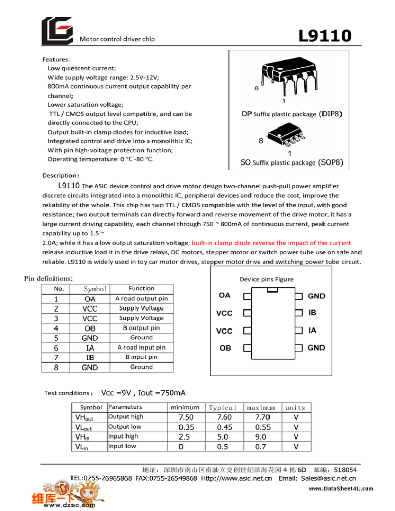
L9110 Motor control driver chip Features: Low quiescent current; Wide supply voltage range: 2.5V-12V; 800mA continuous current output capability per channel; Lower saturation voltage; TTL / CMOS output level compatible, and can be directly connected to the CPU; Output built-in clamp diodes for inductive load; Integrated control and drive into a monolithic IC; With pin high-voltage protection function; Operating temperature: 0 ℃ -80 ℃. DP Suffix plastic package (DIP8) SO Suffix plastic package (SOP8) Description: L9110 The ASIC device control and drive motor design two-channel push-pull power amplifier discrete circuits integrated into a monolithic IC, peripheral devices and reduce the cost, improve the reliability of the whole. This chip has two TTL / CMOS compatible with the level of the input, with good resistance; two output terminals can directly forward and reverse movement of the drive motor, it has a large current driving capability, each channel through 750 ~ 800mA of continuous current, peak current capability up to 1.5 ~ 2.0A; while it has a low output saturation voltage; built-in clamp diode reverse the impact of the current release inductive load it in the drive relays, DC motors, stepper motor or switch power tube use on safe and reliable. L9110 is widely used in toy car motor drives, stepper motor drive and switching power tube circuit. Device pins Figure Pin definitions: No. 1 2 3 4 5 6 7 8 Function Symbol A road output pin OA Supply Voltage VCC Supply Voltage VCC B output pin OB Ground GND A road input pin IA B input pin IB Ground GND OA GND VCC IB VCC IA GND OB Test conditions: Vcc =9V , Iout =750mA Symbol Parameters Output high VHout Output low VLout Input high VHin Input low VLin minimum 7.50 0.35 2.5 0 Typical 7.60 0.45 5.0 0.5 maximum 7.70 0.55 9.0 0.7 units V V V V 地址:深圳市南山区南油立交创世纪滨海花园 4 栋 6D 邮编:518054 TEL:0755-26965868 FAX:0755-26549868 Http://www.asic.net.cn Email: Sales@asic.net.cn L9110 Motor control driver chip Electrical characteristics: Logical relationship: Symbol Parameters Range Min VCC Idd Iin IC IMax Supply Voltage 2.5 Quiescent Current - Operating current 200 Continuous 750 Current peak - Typical 6 0 350 800 1500 Max 12 2 500 850 2000 Units IA H L L H V uA uA mA mA IB L H L H OA H L L L OB L H L L Pin waveform diagram: input A input B output A output B Application Circuit: VCC + DC motor Forward signal L9110 M backward signal GND 地址:深圳市南山区南油立交创世纪滨海花园 4 栋 6D 邮编:518054 TEL:0755-26965868 FAX:0755-26549868 Http://www.asic.net.cn Email: Sales@asic.net.cn
