EECE 277 FPGA Design Topics EECE 277 Course Philosophy [1
advertisement
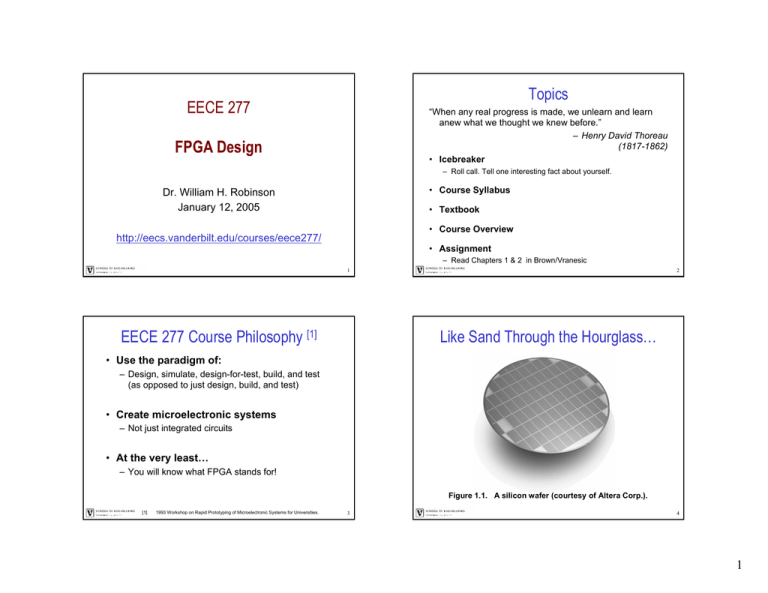
Topics EECE 277 “When any real progress is made, we unlearn and learn anew what we thought we knew before.” – Henry David Thoreau (1817-1862) • Icebreaker FPGA Design – Roll call. Tell one interesting fact about yourself. • Course Syllabus Dr. William H. Robinson January 12, 2005 • Textbook • Course Overview http://eecs.vanderbilt.edu/courses/eece277/ • Assignment – Read Chapters 1 & 2 in Brown/Vranesic 1 EECE 277 Course Philosophy [1] 2 Like Sand Through the Hourglass… • Use the paradigm of: – Design, simulate, design-for-test, build, and test (as opposed to just design, build, and test) • Create microelectronic systems – Not just integrated circuits • At the very least… – You will know what FPGA stands for! Figure 1.1. A silicon wafer (courtesy of Altera Corp.). [1] 1993 Workshop on Rapid Prototyping of Microelectronic Systems for Universities. 3 4 1 Amazing Underlying Technology Change Moore’s Law The number of transistors on a chip doubles every 18 months Gordon E. Moore, Intel co-founder • Empirical observation • Self-fulfilling prophecy • “Cramming More Components onto Integrated Circuits” – Gordon Moore, Electronics, 1965 Adapted from John Kubiatowicz’s CS 252 lecture notes. Copyright © 2003 UCB. 5 6 Projecting the Future PLD vs. ASIC • Programmable Logic Device (PLD) – – – – Simple PLDs (SPLDs) Complex PLDs (CPLDs) Characterized by an AND/OR plane implementation Do not support large or complex functions • Application-Specific Integrated Circuit (ASIC) – Gate arrays, Structured ASICs, Standard Cells, Full Custom – Usually costly in design/fabrication – Textbook by Michael John Sebastian Smith – http://iroi.seu.edu.cn/books/asics/ASICs.htm • Semiconductor Industry Association (SIA) – Predicts the minimum size of a transistor that can be fabricated on an IC 7 8 2 Bridging the Gap What are FPGAs Old Navy Banana Republic PLDs ASICs The GAP SPLDs “Field programmable gate arrays (FPGAs) are digital integrated circuits (ICs) that contain configurable (programmable) blocks of logic along with configurable interconnects between these blocks.” [1] Group of 8 logic cells Gate Arrays CPLDs Memory block Structured ASICs Standard Cell Full Custom Interconnection wires 9 [1] Clive “Max” Maxfield, The Design Warrior’s Guide to FPGAs. Copyright © 2004. 10 Design Process The System Design Process • May be part of larger product design • Major levels of abstraction: – – – – – Specification Architecture Logic design Circuit design Layout FPGA-based system design FPGA-Based System Design: Chapter 1 Copyright 2004 Prentice Hall PTR 11 12 3 Top-Down vs. Bottom-Up Design Design Abstractions • Top-down design adds functional detail. English – Create lower levels of abstraction from upper levels Executable program • Bottom-up design creates abstractions from low-level behavior. function Sequential machines Logic gates • Good design needs both top-down and bottom-up efforts. FPGA-Based System Design: Chapter 1 Copyright 2004 Prentice Hall PTR 13 Course Topics specification behavior Throughput, design time registertransfer Function units, clock cycles logic transistors circuit rectangles layout FPGA-Based System Design: Chapter 1 cost Literals, logic depth nanoseconds microns Copyright 2004 Prentice Hall PTR 14 Laboratory Assignments • Computer-Aided Design (CAD) tools • Altera University Program – For design, placement, and routing • UP2 Design Laboratory Kit • Hardware Description Languages (HDL) – For simulation and synthesis • Rapid Prototyping of Digital Systems • State machines • Teams of 2 – Specification, design, and simulation 15 16 4 Final Project Take a Moment… • Builds on skills from laboratory assignments • Write down your thoughts/reactions to our first day – Anonymous feedback • Implements a “system” on the UP2 – http://microsys6.engr.utk.edu/ece/bouldin_courses/551/551_projects.html • I will stay a few minutes for additional questions • Improve written communication skills • Reading assignment for Friday: – Final report – Brown/Vranesic Ch. 1 & 2 • Improve oral communication skills – Presentation and demo 17 18 5
