Field Effect Transistors
advertisement
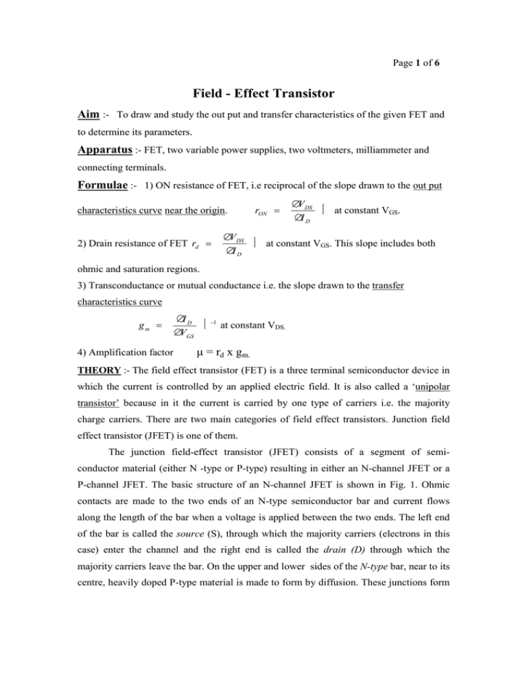
Page 1 of 6 Field - Effect Transistor Aim :- To draw and study the out put and transfer characteristics of the given FET and to determine its parameters. Apparatus :- FET, two variable power supplies, two voltmeters, milliammeter and connecting terminals. Formulae :- 1) ON resistance of FET, i.e reciprocal of the slope drawn to the out put characteristics curve near the origin. 2) Drain resistance of FET rd = rON = ∆VDS Ω at constant VGS. ∆I D ∆VDS Ω at constant VGS. This slope includes both ∆I D ohmic and saturation regions. 3) Transconductance or mutual conductance i.e. the slope drawn to the transfer characteristics curve gm = 4) Amplification factor ∆I D Ω −1 at constant VDS. ∆VGS µ = rd x gm. THEORY :- The field effect transistor (FET) is a three terminal semiconductor device in which the current is controlled by an applied electric field. It is also called a ‘unipolar transistor’ because in it the current is carried by one type of carriers i.e. the majority charge carriers. There are two main categories of field effect transistors. Junction field effect transistor (JFET) is one of them. The junction field-effect transistor (JFET) consists of a segment of semiconductor material (either N -type or P-type) resulting in either an N-channel JFET or a P-channel JFET. The basic structure of an N-channel JFET is shown in Fig. 1. Ohmic contacts are made to the two ends of an N-type semiconductor bar and current flows along the length of the bar when a voltage is applied between the two ends. The left end of the bar is called the source (S), through which the majority carriers (electrons in this case) enter the channel and the right end is called the drain (D) through which the majority carriers leave the bar. On the upper and lower sides of the N-type bar, near to its centre, heavily doped P-type material is made to form by diffusion. These junctions form Page 2 of 6 two P-N diodes and are called the gate (G), which control the carrier flow. The region of N-type material between the two gate regions is called channel through which the majority carriers move from source to drain. The source, drain, and gate terminals in FET are similar to that of emitter, collector and base terminals, respectively, in case of BJT. The source and drain terminals are interchangeable i.e., either end can be used as source and the other end as drain. The voltage between the gate and source is such that the gate is reverse biased. Fig. 1 The P-channel JFET is similar in construction that it uses P-Type bar and two Ntype junctions. The majority carriers in this case are holes which flow through the channel. Schematic symbols for N-channel and P-channel JFETs are shown in Fig.2. The vertical line in the symbol represents the channel to which source S and drain D are connected. The gate arrow always points to N-type material. Fig. 2 Page 3 of 6 The application of a voltage VDS (VDD = drain supply voltage) from drain to source will cause the electrons to flow through the channel. The amount of drain current ID will be determined initially by the value of VDS, since it is just the ohmic resistance of the bar from S to D. Suppose the P-N junctions between gate and source are applied reverse-bias. These two reverse biased P-N junctions develop depletion regions, as shown by the crosshatching in Fig. 1. The depletion regions are non-conductive. As the reverse bias is increased, the size of the depletion regions increases and the drain current is reduced. When the reverse current is large enough for the two depletion regions to meet, the channel becomes pinched off and the drain current cuts off. The reverse bias required for pinch off is called as pinch off voltage Vp. Thus the drain current through the channel depends upon the degree to which the electric field applied to the channel which decreases the conductance of the transistor. Hence the name ‘field-effect transistor (FET)’ given to this device. Description :- To study the out put and transfer characteristics the circuit is connected as shown in Fig. 3. Here the FET is n-channel FET. The source S is grounded. The drain D is connected to a voltage source VDD such that it applies a potential VDS between source and drain, to pull the electrons from the source to the drain. The potential VDS and the drain current ID can be measured from the volt meter and milliammeter connected in the circuit respectively. The gate G is connected to a voltage source VGG such that it applies a reverse bias potential VGS between the gate and source. The potential VGS can be measured from the voltmeter, connected across the gate and source. Fig . 3 Page 4 of 6 Procedure :-The circuit is connected as shown in Fig. 3, to study the out put and transfer characteristics. Output or drain characteristics : Keeping VGS fixed at some value, the drain source voltage (VDS) is changed in steps and corresponding drain current ID is noted in the table 1. A group of such drain characteristics curves are drawn by setting VGS at a different fixed values ( 0V, -1V, -2V etc.). Fig. 4 shows out put or drain characteristics. Graph-1 :- A graph is drawn by taking drain voltage VDS on X-axis and drain current ID on Y-axis by keeping VGS constant. The same graph is drawn for different values of VGS. From these curves we calculate the FET parameters i.e ON resistance (rON) and drain resistance (rd) as shown in the Fig.4. Fig. 4 For low values of VDS, drain current ID varies directly with voltage following Ohm's law. Thus JFET behaves like an ordinary resistor till point A, called knee point, is reached. As VDS further increases, drain current becomes constant at IDSS (maximum drain current). The drain source voltage above which drain current becomes constant is called the pinch off voltage (VP) and the point B is called pinch off point. The region BC is called saturation region or pinch off region. If VDS is increased beyond avalanche breakdown voltage VA corresponding to point C, JFET enters the breakdown region Page 5 of 6 where small changes in VDS produce very large changes in ID. It is due to the avalanche breakdown of reverse-biased gate-channel P-N junction. Transfer characteristics : It is a plot of 1D versus VGS for a fixed value of VDS and is shown in Fig. 5. To get the characteristics, VDS is kept fixed while VGS is varied in steps and the corresponding ID is noted in the table 2. Graph-2 :- A graph is drawn in the 2nd quadrant by taking gate voltage VGS on negative X-axis and drain current ID on Y-axis by keeping VDS constant. The same graph is drawn for different values of VDS. From these curves we calculate the transconductance of FET(gm) as shown in the Fig.5. The pinch-off voltage (VP) can also be known from this graph. Fig. 5 Precautions :- 1) Precautions :- 1) Check the continuity of the connecting terminals before going to connect the circuit. 2) Identify the source, drain and gate terminals of the FET properly before connecting it in the circuit. 3) While taking the readings in the table-1(for out put characteristics) VDS should also be increased after ID attaining saturation value. Page 6 of 6 Results :- 1) Short gate drain current IDSS, i.e. saturation drain current for VGS = 0V. IDSS = mA 2) Pinch off voltage VP, i.e. the minimum VDS for saturation drain current. VP = 3) ON resistance of FET rON = ∆VDS QR = = ∆I D PQ V Ω , at constant VGS. i.e the reciprocal of the slope drawn to the out put characteristics near the origin. ∆VDS TU = = ∆I D ST 4) Drain resistance of FET rd = Ω at constant VGS. The reciprocal of the slope includes both ohmic and saturation regions. 5) Transconductance or mutual conductance ∆I D AB = = ∆VGS BC gm = Ω −1 at constant VDS. i.e. the slope drawn to the transfer characteristics 6) Amplification factor µ = rd x gm = Table-1 Table-2 Out put characteristics VDS V ID VGS2 = VDS VDS1 = V ID (Volt) (mA) (Volt) (mA) S.No. S.No. VGS1 = Transfer characteristics ***** VGS (V) VDS2 = (V) ID ID (Volt) (mA) VGS (Volt) (mA)
