ACPL-352J
Panasonic X-GaN Transistor
Reference Design
1. Introduction
2. Advantages of GaN
Gallium Nitride (GaN) power semiconductors are rapidly
emerging into the commercial market delivering huge benefits
over conventional Silicon-based power semiconductors. GaN
can improve overall system efficiency with lower on-resistance
and the higher switching capability can reduce the overall
system size and costs. The technical benefits coupled with
lower costs have increased the fast adoption of GaN power
semiconductors in applications like industrial power supplies
and renewable energy inverters.
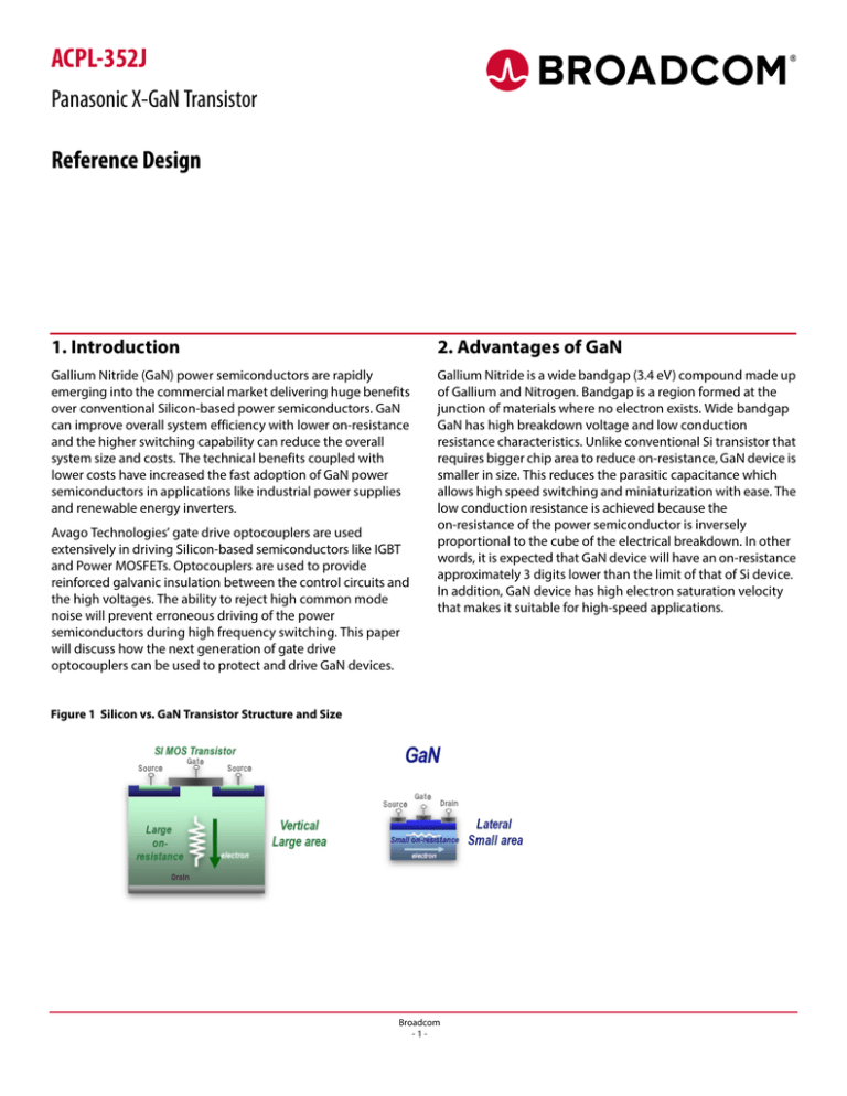
Gallium Nitride is a wide bandgap (3.4 eV) compound made up
of Gallium and Nitrogen. Bandgap is a region formed at the
junction of materials where no electron exists. Wide bandgap
GaN has high breakdown voltage and low conduction
resistance characteristics. Unlike conventional Si transistor that
requires bigger chip area to reduce on-resistance, GaN device is
smaller in size. This reduces the parasitic capacitance which
allows high speed switching and miniaturization with ease. The
low conduction resistance is achieved because the
on-resistance of the power semiconductor is inversely
proportional to the cube of the electrical breakdown. In other
words, it is expected that GaN device will have an on-resistance
approximately 3 digits lower than the limit of that of Si device.
In addition, GaN device has high electron saturation velocity
that makes it suitable for high-speed applications.
Avago Technologies’ gate drive optocouplers are used
extensively in driving Silicon-based semiconductors like IGBT
and Power MOSFETs. Optocouplers are used to provide
reinforced galvanic insulation between the control circuits and
the high voltages. The ability to reject high common mode
noise will prevent erroneous driving of the power
semiconductors during high frequency switching. This paper
will discuss how the next generation of gate drive
optocouplers can be used to protect and drive GaN devices.
Figure 1 Silicon vs. GaN Transistor Structure and Size
Broadcom
-1-
ACPL-352J
Reference Design
2. Advantages of GaN
Power semiconductor is the key device and works on
tremendous amount of power during electrical energy
conversion. It is therefore important to optimize the efficiency
of this device to minimize energy loss during their operation.
GaN is the next generation power semiconductor able to
minimize power loss with the following characteristics:
miniaturization, high breakdown voltage and high-speed
switching.
Figure 2 Panasonic X-GaN™ Transistor Structure
Most of the GaN devices are however normally on which
means the source and drain are conducting when no voltage is
applied at the gate. To stop the conduction, a negative voltage
must be used to reverse the conduction channel. A normally on
transistor poses danger to the system if the gate is not
controlled properly and silicon transistor which is normally off
is more suitable for hazardous high voltage application.
To speed up GaN adoption, Panasonic's X-GaN™ employed a
normally off Gate Injection Transistor (GIT) structure by using P
type GaN gate and diffuse AlGaN channel under the gate. At
the same time, the P type GaN add holes near the drain which
recombines with the electrons at high voltage. This method
solves current collapse problem whereby electrons trapped
near the channel during high voltage increases the transistor
on-resistance. If the increase of on-resistance is not controlled,
the GaN device will overheat and destroy over time. Panasonic
GaN transistors are capable of no current collapse for up
to 850V.
Panasonic has done a concept demo of the world's smallest
400W class All-In-One power supply. The power conversion
stages, PFC and LLC operate at 100 kHz and 280 kHz
respectively. The high frequencies reduce the cost and size of
the power supply by more than 30%. The miniaturized power
supply is measured 11.2cm × 4.95cm × 3.95cm and with
effective power density of 1.83W/cm3. It also achieved a high
conversion efficiency of 94% with the low switching and
conduction losses.
Figure 3 Panasonic World’s Most Compact 400W Power Supply with 94% Conversion Efficiency
Broadcom
-2-
ACPL-352J
Reference Design
3. GaN Market and Adoption
3. GaN Market and Adoption
GaN technology is now widely recognized as a reliable
alternative to silicon. Recent financial investments into GaN
startups like GaN Systems and Transphorm and corporate
partnership between Infineon and Panasonic indicate market
confidence in GaN devices. GaN has huge Total Accessible
Market (TAM) like PF, EV/HEV and PV inverter is one of the
earliest adopters of GaN. In 2014, Yaskawa Electric Corp
launched the world's first PV inverter using a GaN-based power
semiconductor. The PV inverter has the ability to operate
without cooling fans, is 60% the volume of competing devices
and with an overall peak efficiency above 98%.
Avago gate drive optocouplers have been used extensively in
driving Silicon-based semiconductors like IGBT. This paper will
discuss how the improvements in the next generation of gate
drive optocouplers can also be used to drive and protect GaN
devices.
4. GaN Transistor and Gate Drive
Optocouplers
To determine suitable gate driver for GaN operation, Broadcom
evaluated gate drive optocoupler ACPL-352J with Panasonic
GaN transistor, PGA26E19BA using a 100-150V, 5A chopper
board at 100 kHz.
The ACPL-352J is industry's highest output current, 5A smart
gate drive optocoupler. The high peak output current, together
with wide operating voltage make it ideal for driving GaN
transistor directly. The device features fast propagation delay
of 100ns with excellent timing skew performance and has very
high common mode transient immunity (CMTI) of more than
50kV/μs. It can provide GaN with over current protection and
fail-safe functional safety reporting. This full-featured gate
drive optocoupler comes in a compact, surface-mountable
SO-16 package. It provides the reinforced insulation certified
by safety regulatory IEC/EN/DIN, UL and CSA.
The PGA26E19BA is a 600V, 10A GaN enhancement mode
transistor. It uses Panasonic's proprietary Gate Injection
Transistor (GIT) technology to achieve normally off operation
with single GaN device. This extremely high switching speed
X-GaN is capable of no current collapse for up to 850V and has
zero recovery loss characteristic.
Figure 4 100–150V, 5A Chopper Bard with ACPL-352J and PGA26E19BA
Broadcom
-3-
ACPL-352J
Reference Design
5. Driving GaN Transistor
5. Driving GaN Transistor
Figure 5 ACPL-352J Driving Circuit for GaN Transistor
ACPL-352J
Figure 5 shows the ACPL-352J gate drive outputs,
VOUTP/MClamp and VOUTN and external resistors and capacitor
for switching the GaN transistor. The full chopper board
schematic can be found in Figure 11.
Figure 7 GaN Transistor VGS vs. Qg Characteristic
Figure 6 GaN Transistor Gate Current and Voltage Switching
Waveform
VGS
Charging
IG
On State Current
Discharging
The initial in-rush charging current to turn on the GaN quickly
is provided by ACPL-352J VOUTP and the peak current limited
by R9. C16 is used to turn on the GaN faster by increase the
charging current momentarily. The required IG_CHARGE can be
calculated by the GaN's Qgd and turn on time t, for example
10ns.
The "speed-up" capacitor, C16 can be calculated using the Qg
characteristic graph which shows the gate charge needed to
turn on the GaN is 4.5nC.
Equation 1
C16 > Qg / (VCC–VGS–V(neg)) = 4.5nC / (24V – 3.6V-5V) = 292pF
IG_CHARGE = Qgd / t = 4.5nC / 10ns = 450mA
The value of R9 can then be calculated by the gate drive supply,
VCC, GaN gate plateau voltage, Vplateau and IG_CHARGE:
Equation 3
A higher C16, 1nF is chosen to ensure more accumulation
charge for faster turn on.
R9 = (VCC – Vplateau) / IG_CHARGE = (24V – 2.9V) / 450mA = 46
The GaN transistor would require 4.75mA on state current to
continuously bias the VGS diode at 3.6V to maintain the
transistor in on state. This is provided VOUTP and the value of
R15 can be calculated:
51 is selected for R9.
Equation 4
Equation 2
R15 = (VCC – VGSF) / IG_ONSTATE = (24V – 3.6V) / 4.75mA = 4.3k
4.3k is selected for R15.
Broadcom
-4-
ACPL-352J
Reference Design
6. Protecting GaN Transistor
Switching off or discharging the gate of the GaN is done by ACPL-352J's VOUTN and R10. ACPL-352J is connected to a bi-directional
power supply and gate is discharge through VOUTN to –9V. At the same time, the active Miller clamp (Mclamp) will turn on when the
gate discharge to –7V. GaN transistor has very low typical gate threshold voltage of 1.2V. The negative gate voltage and active
Miller clamp help to hold the transistor in off state and shunt parasitic Miller current to prevent false turn on. The peak discharging
gate current can be calculated:
Equation 5
IG_DISCHARGE = (VGSF– VEE2) / R10 = (3.6V – (–9V)) / 27 = 0.467A
6. Protecting GaN Transistor
Figure 8 ACPL-352J Over Current Protection Circuit for GaN Transistor
ACPL-352J
The drain-source voltage of the GaN is monitored by ACPL-352J's OC pin through high voltage blocking diode D2. The chopper is
designed to operate at 5A and over current threshold is set at 7A. When over current occurs, the VDS of the GaN increases to about
0.8V. ACPL-352J has an internal over current threshold voltage, VOC of 9V. The threshold of the over current detection can then be
set by Zener diode, Z2.
Equation 6
Z2 = VOC – VD2 – VDS_OVERCURRENT = 9 – 0.7 – 0.8 = 7.5V
During over current, if the GaN is shutdown abruptly, high overshoot voltage induced by the load or any parasitic inductance can
develop across the drain and source of the GaN. The overshoot will damage the GaN if it exceeds the breakdown voltage. To
minimize such damaging overshoot voltage, ACPL-352J's pin 13, SS does a soft shutdown when over current is detected. GaN gate
voltage is slowly reduced to low level off-state. The rate of soft shutdown can be adjusted through external transistor Q1 and
resistor R8 to reduce the overshoot voltage.
The entire over current protection is completed by reporting the /Fault through the insolated feedback path to the controller.
Beside over current fault, the ACPL-352J also reports high side under voltage lockout fault (/UVLO) and GaN gate status fault
(/Gfault).
Broadcom
-5-
ACPL-352J
Reference Design
7. Chopper Board Switching Performance
Figure 9 ACPL-352J Functional Safety Fault Reporting
ACPL-352J
7. Chopper Board Switching Performance
The chopper board is designed to switch the X-GaN transistor at 100kHz with DC bus voltage from 100-150V. The GaN nominal
working drain current is 5A and over current threshold is set at 7A. Figure 10 shows the switching waveforms of the GaN VGS, VDS,
and IDS. As the chopper board is not connected to any load to dissipate the energy, IDS increases on very switching pulse and
eventually triggers the ACPL-352J's VOC, over current detection threshold. The waveform on the right zooms into the soft shutdown
process once over current is detected.
Figure 10 Chopper Board Switching Performance, Over Current Detection and Soft Shutdown
100kHz, High Frequency Switching
Over Current Detection and Soft Shutdown
VGS, +4/-9V
Over Current > 7A Detected
Soft Shutdown
VDS, 100V
IDS > 7A
I DS
VOC > 9V or
VGaN _DS > 0.8V
VOC (Over
Current
Detection)
Broadcom
-6-
ACPL-352J
Reference Design
8. Other Design Considerations
8. Other Design Considerations
Figure 11 Chopper Board Schematic
The ACPL-352J is powered by a RECOM Econoline DC/DC converter REC3.5-0512DRW. It is a 3.5W regulated converter and provides
up to 10kVDC of reinforced isolation. The 24V dual output is split by a 15V Zener diode Z1 to provide bi-directional gate voltage of
+15 for turning on and –9V for turning off.
Active clamping is provided by TVS diode TVS2, D5 and R14 to clamp the VDS of the GaN from exceeding 300V. 15V Bi-directional
TVS diode TVS1is used to protect the gate of the GaN transistor. Schottky diode D3 is used to clamp negative transient at
ACPL-352J's VOC to prevent any false fault triggering.
Broadcom
-7-
ACPL-352J
Reference Design
9. Bill of Material
9. Bill of Material
Designator
Descriptions
Manufacture Name
Manufacturer Part Number
C1, C6, C8
CAPACITOR, X7R, 1206, 50V, 1μF
MULTICOMP
MCSH31B105K500CT
C3, C4,C5
CAPACITOR, 0805, 1nF, 25V
TDK Corporation
C2012C0G1E103J060AA
C9, C14
Capacitor F X7R 100nF 50V 10%
KEMET
C1206C104K5RACTU
C10
CAPACITOR, X7R, 1206, 50V, 100pF
Samsung-Electro
CL31C101JBCNNNC
C11, C12, C15
Capacitor MLCC X7R 10μF 25V 10%
TAIYO YUDEN
TMK316B7106KL-TD
C13
Capacitor F X7R 10nF 50V 10%
Murata Electronics
GRM3195C1H113JA01D
C16
Capacitor X7R 1nF 50V 10%
YAGEO (PHYCOMP)
CC0805KRX7R9BB152
C17a,b,c
Capacitor Metal Film 450VDC 2.2μF
Panasonic
ECW-FE2W225K
C18a,b,c
Capacitor X7T, 630V, 0.47μF
TDK Corporation
C5750X7T2J474K
D1
DIODE, Schottky, 1200V
Cree Inc.
C4D08120E
D2
Diode, FRD, 1000V
VISHAY
US1M-E3/5AT
D3, D4
DIODE, SCKY RECTI
MULTICOMP
BAT42W
D5
DIODE, SCKY RECTI
DIODES INC.
B140-13-F
D6
DIODE, SCKY RECTI
NXP
PMEG4050EP
Z1
Diode, Zener 15V
DIODES INC.
BZT52C15V
Z2
Diode, Zener 7V5
DIODES INC.
BZT52C7V5
BR1
Diode, Bridge AC230V
MULTICOMP
DB103S
TVS1
TVS 15V bidirectional
Fairchild
SMBJ15CA
TVS2
TVS 300V unidirectional
Littelfuse Inc.
SMCJ300A
R1, R2
RESISTOR, 0805, 330 OHM, 5%
Stackpole
RMCF0805JT330R
R3, R4, R5, R13
RESISTOR, 0805, 10k OHM, 5%
Stackpole
RMCF0805JT10K0
R6
RESISTOR, 0805, 1k OHM, 5%
Yageo
RC0805JR-071KL
R7
RESISTOR, 0805, 100 OHM, 5%
Panasonic
ERJ-6GEYJ101V
R8
RESISTOR, 0805, 510 OHM, 5%
Yageo
RC0805JR-071KL
R10
RESISTOR, 1210, 27 Ohm, 1W
Rohm
MCR25JZHJ270
R14
RESISTOR, 2512, 5R1 Ohm, 1W
Stackpole
RMCF2512JT5R10
R15
RESISTOR, 0805, 4k3 OHM, 5%
Stackpole
RMCF0805JG4K30
R9
RESISTOR, 2512, 51 OHM, 1W
Stackpole
RMCF2512JT51R0
J1~J2
HEADER, 2.54MM, 2WAY
MOLEX
22-27-2021
CON1
HEADER, 2.54MM, 9WAY
Amphenol FCI
68000-103HLF
CON2
HEADER, 2.54MM, 3WAY
MOLEX
WM4112-ND
CON3
Terminal Block 125Vac 2Way
Phoenix Contact
1725656
CNT1,2,3
Connector, Agilent Probe
Oxley
Consign
CNT4a,b
Fuse Holder
Littelfuse Inc.
01020071Z
U1
Isolated Gate Driver Optocoupler
Broadcom
ACPL-352J
F1
Fuse, Bussman (FNM-1)
Bussman
FNM-1
GaN
Transistor, GaN
Panasonic
PGA26E19BA
SW1
Switch Toggle, SPST
Eaton
8444k4
Broadcom
-8-
Designator
Descriptions
Manufacture Name
Transmore
Manufacturer Part Number
L1
Inductor
Consign
U2
Dc-Dc converter
RECOM ECONOLINE
REC3-0512DRW
Q1
TRANS PNP 40V 1A SOT-89
Diodes Incorporated
FCX591ATA
10. Acknowledgment
Avago would like to thank Aaron Cai (Engineer) and Arnel Herreria (Senior Engineer), GaN Field Application Team, Panasonic
Semiconductor Solutions Singapore for their technical support.
For product information and a complete list of distributors, please go to our web
site: www.broadcom.com.
Broadcom, the pulse logo, Connecting everything, Avago Technologies, and the
A logo are the trademarks of Broadcom in the United States, certain other
countries and/or the EU.
Copyright © 2016 Broadcom. All Rights Reserved.
The term "Broadcom" refers to Broadcom Limited and/or its subsidiaries. For
more information, please visit www.broadcom.com.
Broadcom reserves the right to make changes without further notice to any
products or data herein to improve reliability, function, or design.
Information furnished by Broadcom is believed to be accurate and reliable.
However, Broadcom does not assume any liability arising out of the application
or use of this information, nor the application or use of any product or circuit
described herein, neither does it convey any license under its patent rights nor
the rights of others.
pub-005673 – May 3, 2016

![Structural and electronic properties of GaN [001] nanowires by using](http://s3.studylib.net/store/data/007592263_2-097e6f635887ae5b303613d8f900ab21-300x300.png)


