LB1205 - ON Semiconductor
advertisement
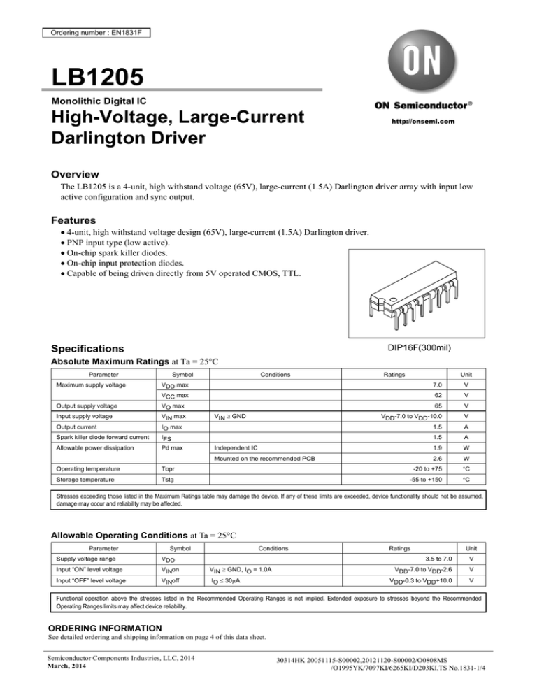
Ordering number : EN1831F LB1205 Monolithic Digital IC High-Voltage, Large-Current Darlington Driver http://onsemi.com Overview The LB1205 is a 4-unit, high withstand voltage (65V), large-current (1.5A) Darlington driver array with input low active configuration and sync output. Features 4-unit, high withstand voltage design (65V), large-current (1.5A) Darlington driver. PNP input type (low active). On-chip spark killer diodes. On-chip input protection diodes. Capable of being driven directly from 5V operated CMOS, TTL. DIP16F(300mil) Specifications Absolute Maximum Ratings at Ta = 25C Parameter Maximum supply voltage Symbol Conditions Ratings Unit VDD max 7.0 VCC max 62 V Output supply voltage VO max 65 V Input supply voltage VIN max VDD-7.0 to VDD-10.0 V Output current IO max 1.5 A Spark killer diode forward current IFS 1.5 A Allowable power dissipation Pd max 1.9 W 2.6 W Operating temperature Topr -20 to +75 C Storage temperature Tstg -55 to +150 C VIN GND Independent IC Mounted on the recommended PCB V Stresses exceeding those listed in the Maximum Ratings table may damage the device. If any of these limits are exceeded, device functionality should not be assumed, damage may occur and reliability may be affected. Allowable Operating Conditions at Ta = 25C Parameter Symbol Conditions Supply voltage range VDD Input “ON” level voltage VINon VIN GND, IO = 1.0A Input “OFF” level voltage VINoff IO 30A Ratings Unit 3.5 to 7.0 V VDD-7.0 to VDD-2.6 V VDD-0.3 to VDD+10.0 V Functional operation above the stresses listed in the Recommended Operating Ranges is not implied. Extended exposure to stresses beyond the Recommended Operating Ranges limits may affect device reliability. ORDERING INFORMATION See detailed ordering and shipping information on page 4 of this data sheet. Semiconductor Components Industries, LLC, 2014 March, 2014 30314HK 20051115-S00002,20121120-S00002/O0808MS /O1995YK/7097KI/6265KI/D203KI,TS No.1831-1/4 LB1205 Electrical Characteristics at Ta 25C, VDD = 5V Ratings Parameter Symbol Conditions Unit min Output saturation voltage typ max VOsat1 VIN = VDD-5.0V, IO = 0.5A 1.2 V VOsat2 VIN = VDD-5.0V, IO = 1.0A 1.5 V 2.0 V mA VOsat3 VIN = VDD-5.0V, IO = 1.5A Output sustain voltage VOsus IO = 100mA Input current IIN VDD = 7.0V, VIN = VDD-7.0V 1.0 Spark killer diode forward voltage VFS IFS = 1.5A 3.0 V Spark killer diode reverse current IRS VCC = 62V, VO = 0V 30 A 65 V Product parametric performance is indicated in the Electrical Characteristics for the listed test conditions, unless otherwise noted. Product performance may not be indicated by the Electrical Characteristics if operated under different conditions. Package Dimensions unit : mm PDIP16 FUSED LEADS / DIP16F (300 mil) CASE 646AQ ISSUE O Pd max -- Ta Allowable power dissipation, Pd max -- W 3.0 2.6 2.5 2.0 1.9 Mounted on the recommended PCB Independent IC 1.56 1.5 1.14 1.0 0.5 0 -20 0 20 40 60 75 80 100 Ambient temperature, Ta -- °C No.1831-2/4 LB1205 Pin Assignment OUT4 IN4 16 15 Recommended PCB VDD GND GND IN3 OUT3 VCC 14 13 12 11 10 9 1 2 3 4 5 6 VCC OUT1 IN1 GND GND IN2 Cu-foiled (GND) 3cm2 7 8 NC OUT2 80×60mm2 Top view Note: VCC (pins 1 and 9) is shorted internally. Equivalent Circuit OUT1 OUT2 OUT3 OUT4 VCC 8kΩ 2kΩ 20kΩ 1.25kΩ 13kΩ VDD GND IN1 IN3 IN4 VOsat -- IO 10 Output saturation voltage, VOsat -- V IN2 7 5 3 2 1.0 7 5 7 0.1 2 3 5 7 1.0 2 3 Output current, IO -- A No.1831-3/4 LB1205 ORDERING INFORMATION Device LB1205-E Package DIP16F(300mil) (Pb-Free / Halogen Free) Shipping (Qty / Packing) LB1205-L-E DIP16F(300mil) (Pb-Free / Halogen Free) 25 / Fan-Fold LB1205L-E DIP16F(300mil) (Pb-Free / Halogen Free) 25 / Fan-Fold LB1205Z-E DIP16F(300mil) (Pb-Free / Halogen Free) 25 / Fan-Fold 25 / Fan-Fold ON Semiconductor and the ON logo are registered trademarks of Semiconductor Components Industries, LLC (SCILLC). SCILLC owns the rights to a number of patents, trademarks, copyrights, trade secrets, and other intellectual property. A listing of SCILLC’s product/patent coverage may be accessed at www.onsemi.com/site/pdf/Patent-Marking.pdf. SCILLC reserves the right to make changes without further notice to any products herein. SCILLC makes no warranty, representation or guarantee regarding the suitability of its products for any particular purpose, nor does SCILLC assume any liability arising out of the application or use of any product or circuit, and specifically disclaims any and all liability, including without limitation special, consequential or incidental damages. “Typical” parameters which may be provided in SCILLC data sheets and/or specifications can and do vary in different applications and actual performance may vary over time. All operating parameters, including “Typicals” must be validated for each customer application by customer’s technical experts. SCILLC does not convey any license under its patent rights nor the rights of others. SCILLC products are not designed, intended, or authorized for use as components in systems intended for surgical implant into the body, or other applications intended to support or sustain life, or for any other application in which the failure of the SCILLC product could create a situation where personal injury or death may occur. Should Buyer purchase or use SCILLC products for any such unintended or unauthorized application, Buyer shall indemnify and hold SCILLC and its officers, employees, subsidiaries, affiliates, and distributors harmless against all claims, costs, damages, and expenses, and reasonable attorney fees arising out of, directly or indirectly, any claim of personal injury or death associated with such unintended or unauthorized use, even if such claim alleges that SCILLC was negligent regarding the design or manufacture of the part. SCILLC is an Equal Opportunity/Affirmative Action Employer. This literature is subject to all applicable copyright laws and is not for resale in any manner. PS No.1831-4/4


