ISL59111
®
Data Sheet
April 19, 2007
FN6172.4
8MHz Rail-to-Rail Composite Video Driver
Features
The ISL59111 is a single rail-to-rail 3-pole output
reconstruction filter with a -3dB roll-off frequency of 8MHz
and a slew rate of 40V/µs, with input signal DC restoration
accomplished with an internal sync tip clamp. Operating
from single supplies ranging from +2.5V to +3.6V and
sinking an ultra-low 2mA quiescent current, the ISL59111 is
ideally suited for low power, battery-operated applications. It
also features inputs capable of reaching down to 0.15V
below the negative rail. Additionally, an enable high pin shuts
the part down in under 14ns.
• 3rd order 8MHz reconstruction filter
The ISL59111 is designed to meet the needs for very low
power and bandwidth required in battery-operated
communication, instrumentation, and modern industrial
applications such as video on demand, cable set-top boxes,
DVD players, and HDTV. The ISL59111 is offered in a
space-saving CSP package guaranteed to a 0.7mm
maximum height constraint and specified for operation from
-40°C to +85°C temperature range.
• Low supply current = 2mA
• Power-down current less than 3µA
• Supplies from 2.5V to 3.6V
• Rail-to-rail output
• Input to 0.15V below VS• Input sync tip clamp
• SAG correction reduces AC coupling capacitor size
• Pb-free plus anneal available (RoHS compliant)
Applications
• Video amplifiers
• Portable and handheld products
• Communications devices
Ordering Information
PART
NUMBER
(See Note)
• 40V/µs slew rate
• Video on demand
PART
MARKING
TAPE &
REEL
PACKAGE
(Pb-Free)
PKG.
DWG. #
• Cable set-top boxes
• Satellite set-top boxes
ISL59111IZ-T7 111Z
7” (3k pcs) 6 Ld CSP (2x3) MDP0054
• DVD players
NOTE: Intersil Pb-free plus anneal products employ special Pb-free
material sets; molding compounds/die attach materials and 100%
matte tin plate termination finish, which are RoHS compliant and
compatible with both SnPb and Pb-free soldering operations. Intersil
Pb-free products are MSL classified at Pb-free peak reflow
temperatures that meet or exceed the Pb-free requirements of
IPC/JEDEC J STD-020.
• HDTV
• Personal video recorders
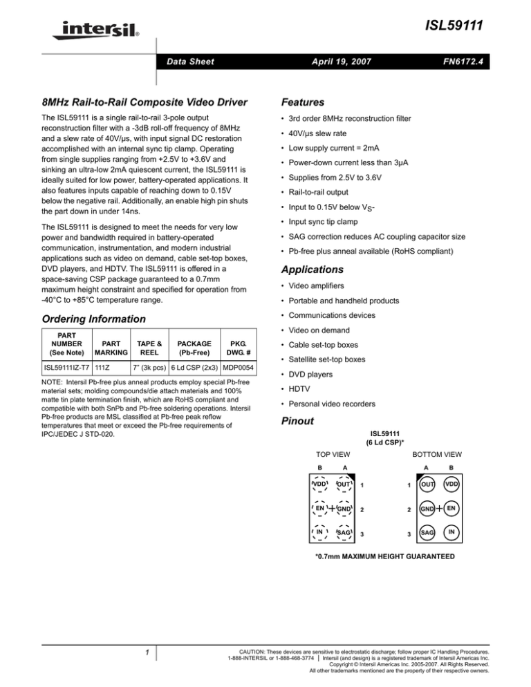
Pinout
ISL59111
(6 Ld CSP)*
TOP VIEW
BOTTOM VIEW
B
A
A
B
VDD
OUT
1
1
OUT
VDD
EN
GND
2
2
GND
EN
IN
SAG
3
3
SAG
IN
*0.7mm MAXIMUM HEIGHT GUARANTEED
1
CAUTION: These devices are sensitive to electrostatic discharge; follow proper IC Handling Procedures.
1-888-INTERSIL or 1-888-468-3774 | Intersil (and design) is a registered trademark of Intersil Americas Inc.
Copyright © Intersil Americas Inc. 2005-2007. All Rights Reserved.
All other trademarks mentioned are the property of their respective owners.
ISL59111
Absolute Maximum Ratings (TA = +25°C)
Supply Voltage from VS+ to GND . . . . . . . . . . . . . . . . . . . . . . . 3.6V
Input Voltage . . . . . . . . . . . . . . . . . . . . . . . VS+ +0.3V to GND -0.3V
Continuous Output Current . . . . . . . . . . . . . . . . . . . . . . . . . . . 40mA
Power Dissipation . . . . . . . . . . . . . . . . . . . . . . . . . . . . . See Curves
Storage Temperature . . . . . . . . . . . . . . . . . . . . . . . .-65°C to +125°C
Ambient Operating Temperature . . . . . . . . . . . . . . . .-40°C to +85°C
Operating Junction Temperature . . . . . . . . . . . . . . . . . . . . . . +125°C
Pb-free reflow profile . . . . . . . . . . . . . . . . . . . . . . . . . .see link below
http://www.intersil.com/pbfree/Pb-FreeReflow.asp
CAUTION: Stresses above those listed in “Absolute Maximum Ratings” may cause permanent damage to the device. This is a stress only rating and operation of the
device at these or any other conditions above those indicated in the operational sections of this specification is not implied.
IMPORTANT NOTE: All parameters having Min/Max specifications are guaranteed. Typ values are for information purposes only. Unless otherwise noted, all tests are
at the specified temperature and are pulsed tests, therefore: TJ = TC = TA
Electrical Specifications
DESCRIPTION
VS+ = 3.3V, TA = +25°C, RL = 150Ω to GND, CL = 0.1µF, unless otherwise specified.
PARAMETER
CONDITIONS
MIN
TYP
MAX
UNIT
3.6
V
2.75
mA
3
µA
INPUT CHARACTERISTICS
VCC
Supply Voltage Range
2.5
IDD-ON
Quiescent Supply Current
VIN = 500mV, EN = VDD, no load
IDD-OFF
Shutdown Supply Current
EN = 0V
VOLS
Output Level Shift Voltage
VIN = 0V, no load
60
130
200
mV
VCLAMP
Input Voltage Clamp
IIN = -1mA
-40
-15
+10
mV
ICLAMP_CHG
Clamp Charge Current
VIN = VCLAMP - 100mV
-6
-3
mA
ICLAMP_DCHG
Clamp Discharge Current
VIN = 500mV
2.5
5
7.5
µA
RIN
Input Resistance
0.5V < VIN < 1.0V
0.5
3
AV
Voltage Gain
RL = 150Ω
1.95
2.0
ASAG
SAG Correction DC Gain to VOUT
SAG open
PSRR
DC Power Supply Rejection
VDD = 2.7V to 3.3V
VOH
Output Voltage High Swing
VIN = 2V, RL = 150Ω to GND
ISC
Output Short-Circuit Current
VIN = 2V, to GND through 10Ω
2
MΩ
2.04
V/V
2.25
V/V
43
63
dB
2.85
3.2
V
-94
VIN = 100mV, out short to VDD through 10Ω
65
115
-3
0
IENABLE
Enable Current
±3.3V, enable pin = 0V
VIL
Disable Threshold
VDD = 2.7V to 3.3V
VIH
Enable Threshold
VDD = 2.7V to 3.3V
1.6
ROUT
Shutdown Output Impedance
EN = 0V DC
3.6
-65
mA
mA
+3
µA
0.8
V
V
4.5
5.9
kΩ
EN = 0V, f = 4.5MHz
3.4
kΩ
AC PERFORMANCE
BW
±0.1dB Bandwidth
RL = 150Ω, CL = 5pF
4
MHz
BW
-3dB Bandwidth
RL = 150Ω, CL = 5pF
8
MHz
Normalized Stopband Gain
f = 27MHz
-24.2
dB
Differential Gain
NTSC and PAL DC coupled
0.10
%
NTSC and PAL AC coupled
0.84
%
NTSC and PAL DC coupled
0.05
°
NTSC and PAL AC coupled
0.62
°
dG
dP
Differential Phase
D/DT
Group Delay Variation
f = 100kHz, 5MHz
5.4
ns
SNR
Signal To Noise Ratio
100% white signal
65
dB
2
FN6172.4
April 19, 2007
ISL59111
Electrical Specifications
DESCRIPTION
VS+ = 3.3V, TA = +25°C, RL = 150Ω to GND, CL = 0.1µF, unless otherwise specified. (Continued)
PARAMETER
CONDITIONS
MIN
TYP
MAX
UNIT
TON
Enable Time
VIN = 500mV, VOUT to 1%
200
ns
TOFF
Disable Time
VIN = 500mV, VOUT to 1%
14
ns
+SR
Positive Slew Rate
10% to 90%, VIN = 1V step
20
41
70
V/µs
-SR
Negative Slew Rate
90% to 10%, VIN = 1V step
-15
-30
-70
V/µs
tF
Fall Time
2.5VSTEP, 80% - 20%
25
ns
tR
Rise Time
2.5VSTEP, 20% - 80%
22
ns
Typical Performance Curves
NORMALIZED GAIN (dB)
0.5
VDD=+3.3V
RL=150Ω
0.3 CL=5pF
-0.1dB BW
@ 4MHz
0.1
-0.1
-0.3
-0.5
100K
1M
10M
FREQUENCY (Hz)
FIGURE 1. GAIN vs FREQUENCY -0.1dB
FIGURE 2. GAIN vs FREQUENCY -3dB POINT
FIGURE 3. GAIN vs FREQUENCY -3dB
FIGURE 4. GAIN vs FREQUENCY FOR VARIOUS RLOAD
3
FN6172.4
April 19, 2007
ISL59111
Typical Performance Curves
FIGURE 5. GAIN vs FREQUENCY FOR VARIOUS CLOAD
FIGURE 6. MAXIMUM OUTPUT MAGNITUDE vs INPUT
MAGNITUDE
FIGURE 8. PSRR vs FREQUENCY
FIGURE 7. PHASE vs FREQUENCY
100
OUTPUT IMPEDANCE (Ω)
VDD=+3.3V
10
1
0.1
0.01
10K
100K
1M
10M
100M
FREQUENCY (Hz)
FIGURE 9. OUTPUT IMPEDANCE vs FREQUENCY
4
FIGURE 10. ISOLATION vs FREQUENCY
FN6172.4
April 19, 2007
ISL59111
Typical Performance Curves
FIGURE 11. MAXIMUM OUTPUT vs LOAD RESISTANCE
FIGURE 12. SUPPLY CURRENT vs SUPPLY VOLTAGE
FIGURE 13. LARGE SIGNAL STEP RESPONSE
FIGURE 14. SMALL SIGNAL STEP RESPONSE
FIGURE 15. ENABLE TIME
FIGURE 16. DISABLE TIME
5
FN6172.4
April 19, 2007
ISL59111
Typical Performance Curves
FIGURE 17. HARMONIC DISTORTION vs FREQUENCY
FIGURE 18. HARMONIC DISTORTION vs OUTPUT VOLTAGE
FIGURE 19. GROUP DELAY vs FREQUENCY
FIGURE 20. -3dB BANDWIDTH vs INPUT RESISTANCE
FIGURE 21. SLEW RATE vs SUPPLY VOLTAGE
6
FN6172.4
April 19, 2007
ISL59111
SYNC CLAMP
VDD
VDD
VDD
SALLEN KEY LOW PASS FILTER
C2
+
CIN
SAG
NETWORK
R1
IN
R2
R3
+
–
IN
RIN
100nF
C1
AC COUPLING
CAPACITOR
VDC
OUT
+
-
C3
C5
47µF
R6
R7 SAG
ROUT
75Ω
C4
RL
75Ω
22µF
R5
EN
EN=GND: SHUTDOWN IDD~0
EN=VDD: ACTIVE IDD~1.5mA
GND
R4
FIGURE 22. BLOCK DIAGRAM
Application Information
The ISL59111 is a single supply rail-to-rail output amplifier
achieving a -3dB bandwidth of around 8MHz and slew rate
of about 40V/µs while demanding only 2mA of supply
current. This part is ideally suited for applications with
specific micropower consumption and high bandwidth
demands. As the performance characteristics above and the
features described below, the ISL59111 is designed to be
very attractive for portable composite video applications.
The ISL59111 features a sync clamp, low pass function, and
SAG network at the output facilitating reduction of typically
large AC coupling capacitors. See Figure 22.
Internal Sync Clamp
The typical embedded video DAC operates from a ground
referenced single supply. This becomes an issue because
the lower level of the sync pulse output may be at a 0V
reference level to some positive level. The problem is
presenting a 0V input to most single supply driven amplifiers
will saturate the output stage of the amplifier resulting in a
clipped sync tip and degrading the video image. A larger
positive reference may offset the input above its positive
range.
The ISL59111 features an internal sync clamp and offset
function to level shift the entire video signal to the best level
before it reaches the input of the amplifier stage. These
features are also helpful to avoid saturation of the output
7
stage of the amplifier by setting the signal closer to the best
voltage range.
The simplified block diagram of the ISL59111 in Figure 22 is
divided into four sections. The first, Section A is the Sync
Clamp. The AC coupled video sync signal is pulled negative
by a current source at the input of the comparator amplifier.
When the sync tip goes below the comparator threshold the
output comparator is driven negative, The PMOS device
turns on clamping sync tip to near ground level. The network
triggers on the sync tip of video signal.
The Sallen Key Low Pass Filter
The Sallen Key is a classic low pass configuration illustrated
in Figure 22. This provides a very stable low pass function,
and in the case of the ISL59111, a three-pole roll-off at
around 8MHz. The three-pole function is accomplished with
an RC low pass network placed in series with and before the
Sallen Key. One pole provided by the RC network and poles
two and three provided by the Sallen Key for a nice threepole roll-off at around 8MHz. If more aggressive, multiplepole roll-offs are needed, multiple ISL59111 can be placed in
series. There will, of course, be a loss of bandwidth as
additional devices are added.
AC Output Coupling and the SAG Network
Composite video signals carry viable information at
frequencies as low as 30Hz up to 5MHz. When a video
system output is AC coupled it is critical that the filter
represented by the output coupling capacitor and the
FN6172.4
April 19, 2007
ISL59111
surrounding resistance network provide a band pass
function with a low pass band low enough to exclude very
low frequencies down to DC, and with a high pass band pass
sufficiently high to include frequencies at the higher end of
the video spectrum.
SAG
NETWORK
AC COUPLING
CAPACITOR
C5
R6
R7
ROUT
RL
C4
R5
R4
Output Drive Capability
The ISL59111 does not have internal short circuit protection
circuitry. If the output is shorted indefinitely, the power
dissipation could easily overheat the die or the current could
eventually compromise metal integrity. Maximum reliability is
maintained if the output current never exceeds ±40mA. This
limit is set by the design of the internal metal interconnect.
Note that in transient applications, the part is robust.
Short circuit protection can be provided externally with a
back match resistor in series with the output placed close as
possible to the output pin. In video applications this would be
a 75Ω resistor and will provide adequate short circuit
protection to the device. Care should still be taken not to
stress the device with a short at the output.
Power Dissipation
FIGURE 23. SAG NETWORK AND AC COUPLING
CAPACITORS
Typically this is accomplished with 220µF coupling capacitor,
a large and somewhat costly solution providing a low
frequency pole around 5Hz. If the size of this capacitor is
even slightly reduced we have found that the accompanying
phase shift in the 50Hz to 100Hz frequency range results in
field tilt resulting in a degraded video image.
The internal SAG network of the ISL59111 replaces the
220µF AC coupling capacitor with a network of two smaller
capacitors as shown in Figure 23. Additionally, the network is
designed to place a zero in the ~30Hz range, providing a
small amount of peaking to compensate the phase response
associated with field tilt.
With the high output drive capability of the ISL59111, it is
possible to exceed the +125°C absolute maximum junction
temperature under certain load current conditions.
Therefore, it is important to calculate the maximum junction
temperature for an application to determine if load conditions
or package types need to be modified to assure operation of
the amplifier in a safe operating area.
The maximum power dissipation allowed in a package is
determined according to:
T JMAX – T AMAX
PD MAX = --------------------------------------------Θ JA
Where:
TJMAX = Maximum junction temperature
DC Output Coupling
TAMAX = Maximum ambient temperature
The ISL59111 internal sync clamp makes it possible to DC
couple the output to a video load, eliminating the need for
any AC coupling capacitors, saving board space and
additional expense for capacitors making the ISL59111 is
designed to be extremely attractive for portable video
applications Additionally, this solution completely eliminates
the issue of field tilt in the lower frequency. The trade off is
greater demand of supply current. Typical load current for
AC coupled is around 3mA compared to typical 6mA used
when DC coupling.
ΘJA = Thermal resistance of the package
The maximum power dissipation actually produced by an IC
is the total quiescent supply current times the total power
supply voltage, plus the power in the IC due to the load, or:
for sourcing:
V OUT
PD MAX = V S × I SMAX + ( V S – V OUT ) × ---------------R
L
for sinking:
ENABLE
+
-
ROUT
PD MAX = V S × I SMAX + ( V OUT – V S ) × I LOAD
TELEVISION
OR VCR
FIGURE 24. DC COUPLE
8
FN6172.4
April 19, 2007
ISL59111
Where:
VS = Supply voltage
ISMAX = Maximum quiescent supply current
VOUT = Maximum output voltage of the application
RLOAD = Load resistance tied to ground
ILOAD = Load current
By setting the two PDMAX equations equal to each other, we
can solve the output current and RLOAD to avoid the device
overheat.
Power Supply Bypassing Printed Circuit Board
Layout
As with any modern operational amplifier, a good printed
circuit board layout is necessary for optimum performance.
Lead lengths should be as short as possible. The power
supply pin must be well bypassed to reduce the risk of
oscillation. For normal single supply operation, a single
4.7µF tantalum capacitor in parallel with a 0.1µF ceramic
capacitor from VS+ to GND will suffice.
Printed Circuit Board Layout
For good AC performance, parasitic capacitance should be
kept to minimum. Use of wire wound resistors should be
avoided because of their additional series inductance. Use
of sockets should also be avoided if possible. Sockets add
parasitic inductance and capacitance that can result in
compromised performance.
9
FN6172.4
April 19, 2007
ISL59111
3x2 Chip Scale Package (CSP)
MDP0054
3x2 CHIP SCALE PACKAGE
E
MILLIMETERS
SYMBOL
MIN
NOMINAL
MAX
A
0.54
0.65
0.70
A1
0.27
0.29
0.31
D
PIN 1 ID
0.36 REF
A2
TOP VIEW
b
θ 0.34
θ 0.37
θ 0.40
D
0.94
0.99
1.04
0.50 BASIC
D1
E
A2
A
A1
SIDE VIEW
1.44
1.49
E1
1.00 BASIC
e
0.50 BASIC
SD
0.25 BASIC
SE
0.00 BASIC
NOTE:
1.54
Rev. 1 2/07
1. All dimensions are in millimeters.
E1
e
SE
B
SD
D1
A
PIN A1
INDICATOR
1
2
3
b
BOTTOM VIEW
All Intersil U.S. products are manufactured, assembled and tested utilizing ISO9000 quality systems.
Intersil Corporation’s quality certifications can be viewed at www.intersil.com/design/quality
Intersil products are sold by description only. Intersil Corporation reserves the right to make changes in circuit design, software and/or specifications at any time without
notice. Accordingly, the reader is cautioned to verify that data sheets are current before placing orders. Information furnished by Intersil is believed to be accurate and
reliable. However, no responsibility is assumed by Intersil or its subsidiaries for its use; nor for any infringements of patents or other rights of third parties which may result
from its use. No license is granted by implication or otherwise under any patent or patent rights of Intersil or its subsidiaries.
For information regarding Intersil Corporation and its products, see www.intersil.com
10
FN6172.4
April 19, 2007
