Supertex inc.
HV9918
Hysteretic, Buck, High Brightness LED Driver
with High-Side Current Sensing
Features
►
►
►
►
►
►
►
►
►
►
General Description
Hysteretic control with high-side current sensing
Integrated 40V 1.0Ω MOSFET
>90% Efficiency
Wide input voltage range: 4.5 to 40V
±5% LED current accuracy
Up to 2.0MHz switching frequency
Adjustable constant LED current
Analog or PWM control signal for PWM dimming
Over-temperature protection
-40ºC to +125ºC operating temperature range
The HV9918 is a PWM controller IC designed to drive high
brightness LEDs using a buck topology. It operates from an input
voltage of 4.5 to 40VDC and employs hysteretic control with a
high-side current sense resistor to set the constant output current
up to 700mA. The device is well suited for applications requiring
a wide input voltage range. The high-side current sensing and an
integrated current-setting circuitry minimize the number of external
components while delivering an accurate average output.
Dedicated pulse-width modulation (PWM) input enables pulsed
LED dimming over a wide range of brightness levels. A hysteretic
control method ensures excellent input supply rejection and fast
response during load transients and PWM dimming.
Applications
►
►
►
►
The HV9918 offers an analog-controlled PWM dimming feature
that reduces the output current by applying an external DC voltage
below the internal 2.0V threshold voltage from ADIM to GND. ADIM
can also accept input from a resistor divider including a negative
temperature coefficient (NTC) thermistor connected between
ADIM and GND, or a positive temperature coefficient (PTC)
thermistor connected between ADIM and VDD thus providing a
PWM thermal-foldback feature that reduces the LED current when
the temperature of the LED string exceeds a specified temperature
point. Additional features include thermal-shutdown protection.
Low voltage industrial and architectural lighting
General purpose constant current source
Signage and decorative LED lighting
Indicator and emergency lighting
The high switching frequency up to 2.0MHz permits the use of
small inductors and capacitors, minimizing space and cost in the
overall system.
The HV9918 comes in a small 8-Lead DFN package and is ideal
for industrial and general lighting applications.
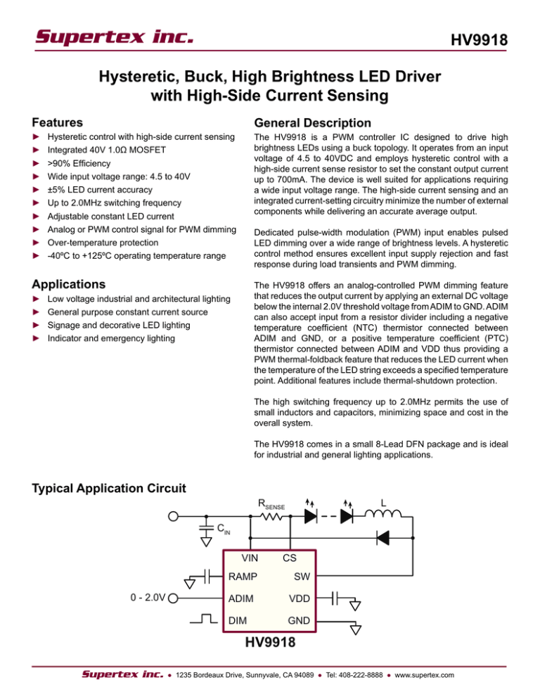
Typical Application Circuit
RSENSE
L
CIN
VIN
0 - 2.0V
CS
RAMP
SW
ADIM
VDD
DIM
GND
HV9918
Supertex inc.
● 1235 Bordeaux Drive, Sunnyvale, CA 94089 ● Tel: 408-222-8888 ● www.supertex.com
HV9918
Pin Description
Ordering Information
Package Options
Device
CS
1
8
SW
VIN
2
7
GND
RAMP
3
6
VDD
ADIM
4
5
DIM
8-Lead DFN
3.00x3.00mm body,
0.80mm height (max),
0.65mm pitch
HV9918
HV9918K7-G
-G indicates package is RoHS compliant (‘Green’)
GND
8-Lead DFN (K7)
(top view)
Product Marking
Parameter
Value
VIN, CS, SW to GND
-0.3 to +45V
VDD, RAMP, DIM, ADIM to GND
-0.3 to +6.0V
CS to VIN
-1.0 to +0.3V
Continuous power dissipation, (TA = +25°C)
Operating temperature range
8-Lead DFN (K7)
Thermal Resistance
1.6W
-40°C to +125°C
Junction temperature
+150°C
Storage temperature range
Y = Last Digit of Year Sealed
W = Code for Week Sealed
L = Lot Number
= “Green” Packaging
9918
YWLL
Absolute Maximum Ratings
Package
θja
8-Lead DFN (K7)
60OC/W
Mounted on FR-4 board, 25mm x 25mm x 1.57mm
-65°C to +150°C
Stresses beyond those listed under “Absolute Maximum Ratings” may cause
permanent damage to the device. These are stress ratings only, and functional
operation of the device at these or any other conditions beyond those indicated in
the operational sections of the specifications is not implied. Exposure to absolute
maximum rating conditions for extended periods may affect device reliability.
Electrical Characteristics
(VIN = 12V, VDIM = VDD, VRAMP = GND, CVDD = 1.0µF, RCS = 0.5Ω, TA = TJ = -40OC to +125OC* unless otherwise noted)
Sym
Description
Min
Typ
Max
Units
VIN
Input DC supply voltage range
4.5
VDD
Internally regulated voltage
-
40
V
DC input voltage
4.5
-
5.5
V
VIN = 6.0 to 40V
Supply current
-
-
1.5
mA
SW = GND
IIN, SDN
Shutdown supply current
-
-
900
µA
DIM < 0.7V
IIN, LIM
Current limit
-
30
-
-
8.0
-
Switchingr frequency
-
-
2.0
MHz
UVLO
VDD Undervoltage lockout threshold
-
-
4.5
V
VDD rising
ΔUVLO
VDD Undervoltage lockout hysteresis
-
500
-
mV
VDD falling
IIN
fSW
mA
Conditions
VIN = 4.5V, VDD = 0V
VIN = 4.5V, VDD = 4.0V
---
* Guaranteed by design and characterization, 100% tested at TA = 25 C. Typical characteristics are given at TA = 25OC.
O
Supertex inc.
● 1235 Bordeaux Drive, Sunnyvale, CA 94089 ● Tel: 408-222-8888 ● www.supertex.com
2
HV9918
Electrical Characteristics
(VIN = 12V, VDIM = VDD, VRAMP = GND, CVDD = 1.0µF, RCS = 0.5Ω, TA = TJ = -40OC to +125OC* unless otherwise noted)
Sym
Description
Min
Typ
Max
Units
Conditions
Sense Comparator
VRS(HI)
Sense voltage threshold high
213
-
246
mV
(VIN - VCS) rising
VRS(LO)
Sense voltage threshold low
158
-
182
mV
(VIN - VCS) falling
tDPDL
Propagation delay to SW off
-
70
-
ns
Rising edge of
(VIN - VCS) = VRS(HI) +70mV to
VSW = 0.9 • VIN
tDPDH
Propagation delay to SW on
-
70
-
ns
Falling edge of
(VIN - VCS) = VRS(LO) -70mV to
VSW = 0.1 • VIN
ICS
Current-sense input current
-
-
1.0
µA
(VIN - VCS) = 200mV
Current-sense threshold hysteresis
-
56
70
mV
---
ICS(HYS)
DIM Input
VIH
Pin DIM input high voltage
2.2
-
-
V
---
VIL
Pin DIM input low voltage
-
-
0.7
V
---
tON
Turn-on time
-
100
-
ns
DIM rising edge to
VSW = 0.9 • VIN
tOFF
Turn-off time
-
100
-
ns
DIM falling edge to
VSW = 0.1 • VIN
Output Switch
IDC
SW continuous current
-
-
0.7
A
---
RON
ON resistance
-
1.0
2.0
Ω
---
ILEAK
SW leakage current
-
10
-
µA
VIN = 40V
128
140
-
ºC
---
-
60
-
ºC
---
130
-
300
550
-
1250
Over-Temperature Protection
TOT
∆THYST
Over temperature trip limit
Temperature hysteresis
Analog Control of PWM Dimming
Hz
CRAMP = 47nF
fRAMP
Dimming frequency
VLOW
RAMP threshold, Low
-
0.1
-
V
---
VHiGH
RAMP threshold, High
1.8
-
2.1
V
---
VOS
ADIM offset voltage
-35
-
35
mV
---
CRAMP = 10nF
* Guaranteed by design and characterization, 100% tested at TA = 25OC. Typical characteristics are given at TA = 25OC.
Supertex inc.
● 1235 Bordeaux Drive, Sunnyvale, CA 94089 ● Tel: 408-222-8888 ● www.supertex.com
3
HV9918
Block Diagram
VIN
VDD
REGULATOR
SW
+
-
CS
CURRENT
SENSE
COMPARATOR
BANDGAP
REF
+
-
DIM
UVLO
COMPARATOR
GND
RAMP
PWM RAMP
0.1~1.9V
ADIM
+
Application Information
General Description
The HV9918 is a step-down, constant current, high-brightness LED (HB LED) driver. The device operates from a 4.5
to 40V input voltage range, and includes an internal 40V
1.0Ω N-channel MOSFET. A high-side current sense resistor
sets the output current and a dedicated PWM dimming input
(DIM) allows for a wide range of diming duty ratios. PWM
dimming can also be achieved by applying a DC voltage between 0 and 2.0V to the analog dimming input (ADIM). In
this case, the dimming frequency can be programmed using
a single capacitor at the RAMP pin. The high-side current
setting and sensing scheme minimizes the number of external components while delivering LED current with ±5%
accuracy using a 1% sense resistor.
HV9918
DIM Input
The HV9918 allows dimming with a PWM signal at the DIM
input. A logic level below 0.7V at DIM halts SW switching,
turning the LED current off. To turn the LED current back on,
the logic level at DIM must be at least 2.2V.
ADIM and RAMP Inputs
The PWM dimming scheme can be also implemented by
applying an analog control signal to ADIM pin. If an analog control signal of 0 ~ 2.0V is applied to ADIM, the device
compares this analog input to a voltage ramp to pulse-widthmodulate the LED current. Connecting an external capacitor
to RAMP programs the PWM dimming ramp frequency.
fPWM =
1
CRAMP • 120kΩ
Undervoltage Lockout (UVLO)
The HV9918 includes a 3.7V under-voltage lockout (UVLO)
with 500mV hysteresis. When VIN falls below 3.7V, switching
of SW is disabled. Switching of SW resumes once VIN is 4.5V
or higher.
DIM and ADIM inputs can be used simultaneously. In such
case, fPWM(MAX) must be selected lower than the frequency of
the dimming signal at DIM. The smaller dimming duty cycle
of ADIM and DIM will determine the SW signal.
5.0V Regulator
VDD is the output of a 5.0V regulator capable of sourcing
8mA. Bypass VDD to GND with a 1.0μF capacitor.
When the analog control of the PWM dimming feature is not
used, RAMP must be wired to GND, and ADIM should be
connected to VDD.
Supertex inc.
● 1235 Bordeaux Drive, Sunnyvale, CA 94089 ● Tel: 408-222-8888 ● www.supertex.com
4
HV9918
One possible application of the ADIM feature of the HV9918
may include protection of the LED load from over-temperature by connecting an NTC thermistor at ADIM, as shown in
Figure 1.
VDD
HV9918
the inductor ramps up and the voltage across the sense resistor reaches the upper threshold, the internal MOSFET at
SW turns off. The MOSFET turns on again when the inductor
current ramps down through the freewheeling diode until the
voltage across the sense resistor equals the lower threshold.
Use the following equation to determine the inductor value
for a desired value of operating frequency fS:
ADIM
L=
NTC
GND
∆IO =
Setting LED Current with External Resistor RSENSE
The output current in the LED is determined by the external
current sense resistor (RSENSE) connected between VIN and
CS. Disregarding the effect of the propagation delays, the
sense resistor can be calculated as:
RSENSE ≈
2
•
(VRS(HI) + VRS(LO) )
ILED
VRS(HI)
RSENSE
=
VRS(HI) - VRS(LO)
RSENSE
∆I = ∆IO +
ILED
TS =
tDPDL
VRS(LO)
RSENSE
(VIN - VOUT )tDPDL VOUT tDPDH
∆IO
∆IO
and tDPDL, tDPDH are the propagation delays. Note, that the current ripple ∆I in the inductor L is greater than ∆IO. This ripple
can be calculated from the following equation:
200mV
Selecting Buck Inductor L
The HV9918 regulates the LED output current using an input
comparator with hysteresis (Figure 2). As the current through
ILED
fSVIN ∆IO
-
where:
Figure 1
1
(VIN - VOUT )VOUT
(VIN - VOUT)tDPDL
L
+
VOUT tDPDH
L
For the purpose of the proper inductor selection, note that
the maximum switching frequency occurs at the highest VIN
and VOUT = VIN/2.
1
fS
tDPDH
ΔI
ΔIO
t
VDIM
Figure 2
Supertex inc.
● 1235 Bordeaux Drive, Sunnyvale, CA 94089 ● Tel: 408-222-8888 ● www.supertex.com
5
t
HV9918
Thermal Shutdown
The HV9918 thermal-shutdown feature turns off the SW driver when the junction temperature exceeds +140°C. The SW
driver turns back on when the junction temperature drops
60°C below the shutdown temperature threshold.
Freewheeling Diode Selection
The forward voltage of the freewheeling diode should be
as low as possible for better efficiency. A Schottky diode
is a good choice as long as the breakdown voltage is high
enough to withstand the maximum operating voltage. The
forward current rating of the diode must be at least equal to
the maximum LED current.
LED Current Ripple
The LED current ripple is equal to the inductor current ripple.
In cases when a lower LED current ripple is needed, a capacitor can be placed across the LED terminals.
PCB Layout Guidelines
Careful PCB layout is critical to achieve low switching losses
and stable operation. Use a multilayer board whenever possible for better noise immunity. Minimize ground noise by
connecting high-current ground returns, the input bypass
capacitor ground lead, and the output filter ground lead to
a single point (star ground configuration). The fast di/dt loop
is formed by the input capacitor CIN, the free-wheeling diode
and the HV9918 switching MOSFET. To minimize noise interaction, this loop area should be as small as possible. Place
RSENSE as close as possible to the input filter and VIN. For
better noise immunity, a Kelvin connection is strongly recommended between CS and RSENSE. Connect the exposed tab
of the IC to a large-area ground plane for improved power
dissipation.
Pin Description
Pin #
Pin
Description
1
CS
Current sense input. Senses LED string current.
2
VIN
Input voltage 4.5 to 40V DC.
3
RAMP
Analog PWM dimming ramp output.
4
ADIM
Analog 0 ~ 2.0V signal input for analog control of PWM dimming.
5
DIM
PWM signal input.
6
VDD
Internally regulated supply voltage. Connect a capacitor from VDD to ground.
7
GND
Device ground.
8
SW
TAB
GND
Open Drain Output of an internal 40V 1.0Ω MOSFET.
Must be wired to pin 7 on PCB.
Supertex inc.
● 1235 Bordeaux Drive, Sunnyvale, CA 94089 ● Tel: 408-222-8888 ● www.supertex.com
6
HV9918
8-Lead DFN Package Outline (K7)
3.00x3.00mm body, 0.80mm height (max), 0.65mm pitch
D2
D
8
8
E
E2
Note 1
(Index Area
D/2 x E/2)
Note 1
(Index Area
D/2 x E/2)
1
1
Top View
Bottom View
View B
Note 3
θ
A
A3
e
b
A1
L
Seating
Plane
L1
Note 2
View B
Side View
Notes:
1. A Pin 1 identifier must be located in the index area indicated. The Pin 1 identifier can be: a molded mark/identifier; an embedded metal marker; or
a printed indicator.
2. Depending on the method of manufacturing, a maximum of 0.15mm pullback (L1) may be present.
3. The inner tip of the lead may be either rounded or square.
Symbol
Dimension
(mm)
A
A1
MIN
0.70
0.00
NOM
0.75
0.02
MAX
0.80
0.05
A3
0.20
REF
b
D
D2
E
E2
e
0.25
2.85*
1.60
2.85*
1.35
0.30
3.00
-
3.00
-
0.35
3.15*
2.50
3.15*
1.75
0.65
BSC
L
L1
θ
0.30
0.00*
0O
0.40
-
-
0.50
0.15
14O
JEDEC Registration MO-229, Variation WEEC-2, Issue C, Aug. 2003.
* This dimension is not specified in the JEDEC drawing.
Drawings not to scale.
Supertex Doc. #: DSPD-8DFNK73X3P065, Version C081109.
(The package drawing(s) in this data sheet may not reflect the most current specifications. For the latest package outline
information go to http://www.supertex.com/packaging.html.)
Supertex inc. does not recommend the use of its products in life support applications, and will not knowingly sell them for use in such applications unless it receives
an adequate “product liability indemnification insurance agreement.” Supertex inc. does not assume responsibility for use of devices described, and limits its liability
to the replacement of the devices determined defective due to workmanship. No responsibility is assumed for possible omissions and inaccuracies. Circuitry and
specifications are subject to change without notice. For the latest product specifications refer to the Supertex inc. (website: http//www.supertex.com)
Supertex inc.
©2010 Supertex inc. All rights reserved. Unauthorized use or reproduction is prohibited.
Doc.# DSFP-HV9918
C092710
1235 Bordeaux Drive, Sunnyvale, CA 94089
Tel: 408-222-8888
www.supertex.com
7
