Analog-to-Digital Conversion Proportional Signals
advertisement
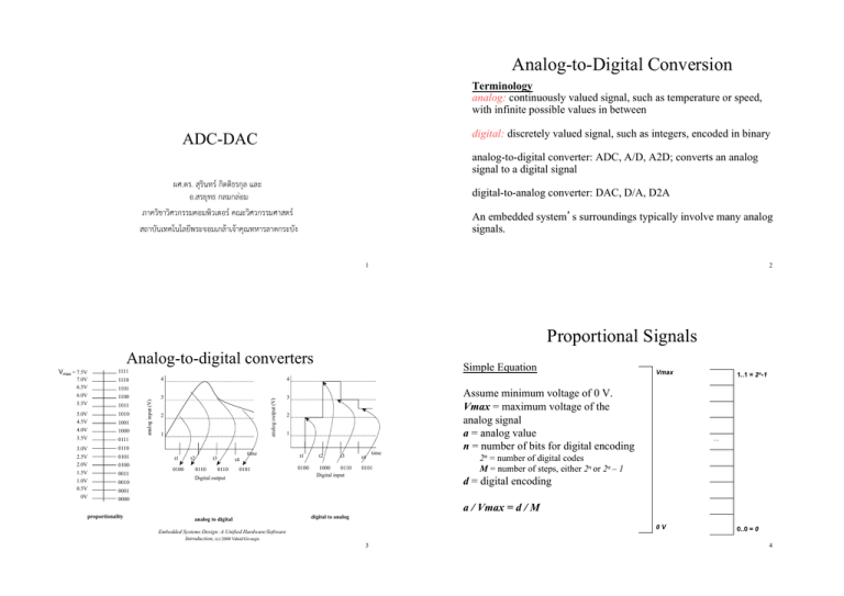
Analog-to-Digital Conversion Terminology analog: continuously valued signal, such as temperature or speed, with infinite possible values in between digital: discretely valued signal, such as integers, encoded in binary ADC-DAC analog-to-digital converter: ADC, A/D, A2D; converts an analog signal to a digital signal ผศ.ดร. สุรินทร์ กิตติธรกุล และ อ.สรยุทธ กลมกล่อม ภาควิชาวิศวกรรมคอมพิวเตอร์ คณะวิศวกรรมศาสตร์ สถาบันเทคโนโลยีพระจอมเกล้าเจ้าคุณทหารลาดกระบัง digital-to-analog converter: DAC, D/A, D2A An embedded system s surroundings typically involve many analog signals. 1 2 Proportional Signals Analog-to-digital converters Simple Equation 1111 7.0V 6.5V 6.0V 5.5V 1110 5.0V 4.5V 4.0V 3.5V 1010 3.0V 2.5V 2.0V 1.5V 1.0V 0.5V 0V 0110 4 4 3 3 1100 1011 1001 1000 0111 0101 0100 0011 0010 analog output (V) 1101 analog input (V) Vmax = 7.5V 2 1 t1 0100 t2 time t3 0110 t4 0110 0101 Digital output 2 1 t1 0100 t2 t3 1000 0110 Digital input t4 time 0101 Vmax Assume minimum voltage of 0 V. Vmax = maximum voltage of the analog signal a = analog value n = number of bits for digital encoding 1..1 = 2n-1 … 2n = number of digital codes M = number of steps, either 2n or 2n – 1 d = digital encoding 0001 0000 proportionality a / Vmax = d / M analog to digital digital to analog 0V Embedded Systems Design: A Unified Hardware/Software Introduction, (c) 2000 Vahid/Givargis 3 0..0 = 0 4 Resolution Let n = 2 Vmax DAC vs. ADC DAC: n digital inputs for digital encoding d analog input for Vmax analog output a 3=11 M = 2n – 1 r 3 steps on the digital scale d0 = 0 = 0b00 dVmax = 3 = 0b11 Vmax x0 x1 … DAC a Xn-1 3=11 ADC: 2=10 M = 2n Given a Vmax analog input and an analog input a, how does the converter know what binary value to assign to d in order to satisfy the ratio? 2=10 4 steps on the digital scale d0 = 0 = 0b00 dVmax - r = 3 = 0b11 (no dVmax ) 1=01 – – 1=01 r, resolution: smallest analog change resulting from changing one bit 0V 0=00 0=00 – may use DAC to generate analog values for comparison with a ADC guesses an encoding d, then checks its guess by inputting d into the DAC and comparing the generated analog output a with original analog input a How does the ADC guess the correct encoding? 5 6 Applications Digital Signal Processing • Audio – Speech recognition – special effects (reverb, noise cancellation, etc) • Video Vref Analog signal (time varying, continuous) 0 – Filtering – Special effects – Compression Incoming samples Analog-toDigital Converter (ADC) 0x030, 0x4A, 0x12, 0xAF, etc. Digital-toAnalog Converter (DAC) 0x0B3, 0x23, 0xCF, µProcessor 0x78, etc. performs computation Time Vref • Data logging new waveform 0 Time 7 Outgoing samples 8 Vocabulary Bit Weight • ADC (Analog-to-Digital Converter) – converts an analog signal (voltage/current) to a digital value • DAC (Digital-to-Analog Converter) – converts a digital value to an analog value (voltage/current) • Sample period – for ADC, time between each conversion Notice the concept of bit weight in the last example: bit 7 = 7.5 V = 15/2 bit 6 = 3.75 V = 15/4 Each bit is weighted with an analog value, such that a 1 in that bit position adds its analog value to the total analog value represented by the digital encoding. – Typically, samples are taken at a fixed rate • Vref (Reference Voltage) – analog signal varies between 0 and Vref, or between +/- Vref • Resolution – number of bits used for conversion (8 bits, 10 bits, 12 bits, 16 bits, etc). • Conversion Time – the time it takes for a analog-to-digital conversion Example: -5 V to +5 V analog range, n=8 Digital Bit Bit Weight (V) 7 10/2 = 5 6 10/4 = 2.5 5 10/8 = 1.25 4 10/16 = 0.625 3 10/32 = 0.313 2 10/64 = 0.157 1 10/128 = 0.078 0 10/256 = 0.039 9 Sample ADC Computations Bit Weight Example (continued): -5 V to +5 V analog range, n=8 Digital numbers for a few analog values – – Values shown increment by 6 bits (weight for bit position 5 is 1.25 V) Maximum digital number only approximates the maximum analog value in the range • Try (-5) + sum of all bit weights 10 Analog (V) Digital (hex) -5 00 -3.75 20 -2.5 40 -1.25 60 0 80 1.25 A0 2.5 C0 3.75 E0 5-0.039 = 4.961 FF If Vref = 5V, and the 10-bit A/D output code is 0x12A, what is the ADC input voltage? output_code/2N * Vref = (0x12A)/210 * 5 V = 298/1024 * 5 V = 1.46 V (Vin) If Vref = 5V, and the upper 8 bits of the A/D output code is 0xA9, what is the ADC input voltage? output_code/2N * Vref = (0xA9)/28 * 5 V = 169/256 * 5 V = 3.3 V (Vin) If Vref = 4V, and the A/D input voltage is 2.35 V, what is the ADC output code, upper 8-bits? 11 Vin/ Vref * 2N = 2.35 V/ 4 V * 28 = .5875 * 256 = 150.4 = 150 = 0x96 12 A 1-bit ADC Vref analog signal Vin R Vref/2 A 2-bit ADC R Vin + - Vdd R + Vout=Vdd is Vin > Vref/2 - Vout=0 if Vin < Vref/2 A 3/4Vref Vin + B - 1/2Vref R Vin + C - R 1/4Vref digital signal R A B C D1 D0 ------------0 0 0 0 0 0 0 1 0 1 0 1 1 1 0 1 1 1 1 1 D[1:0] (other codes don t cares) Encoding logic comparator 13 14 Successive Approximation ADC ADC Architectures First, set DAC to produce Vref/ 2. • The previous architectures are called Flash ADCs Output of Comparator is Q[N-1] (MSB) – Fastest possible conversion time – Requires the most transistors of any architecture – N-bit converter requires 2N-1 comparators. – Commercially available flash converters up to 12 bits. – Conversion done in one clock cycle If MSB =1 , then Vin between Vref and Vref/2, so set DAC to produce ¾ Vref. If MSB=0, then Vin between Vref/2 and 0, so set DAC to ½ Vref. • Successive approximation ADCs – Use only one comparator – Take one clock cycle per bit – High precision (16-bit converters are available) Output of comparator is now Q[N-2]. Do this for each bit. Output is Q[N]. 15 From http://www.allaboutcircuits.com Takes N cycles. 16 ADC, DAC Equations ADC: Digital Encoding ADC: Vin = input voltage, Vref = reference voltage Vref N = number of bits of precision Vin/ Vref * 2N = output_code output_code/ 2N * Vref = Vin Guessing the encoding is similar to finding an item in a list. output code ADC Vin 1. N • 2n comparisons: Slow! 1 LSB = Vref/2N 2. DAC: Vout = output voltage, Vref = reference voltage, N = number of bits of precision Vref 2N Vout/ Vref * = input_code input_code/ 2N * Vref = Vout Sequential search – counting up: start with an encoding of 0, then 1, then 2, etc. until find a match. Vout input code DAC Binary search – successive approximation: start with an encoding for half of maximum; then compare analog result with original analog input; if result is greater (less) than the original, set the new encoding to halfway between this one and the minimum (maximum); continue dividing encoding range in half until the compared voltages are equal • n comparisons: Faster, but more complex converter N 1 LSB = Vref/2N ! Takes time to guess the encoding: start conversion input, conversion complete output 17 18 ADC using successive approximation ADC using successive approximation • Given an analog input signal whose voltage should range from 0 to 15 volts, and an 8-bit digital encoding, calculate the correct encoding for 5 volts. Then trace the successive-approximation approach to find the correct encoding. • Assume M = 2n – 1 a / Vmax = d / M 5 / 15 = d / (256 - 1) d = 85 or binary 01010101 Step 1-4: determine bits 0-3 ½(Vmax – Vmin) = 7.5 volts Vmax = 7.5 volts. 0 0 0 0 0 0 0 0 ½(7.5 + 0) = 3.75 volts Vmin = 3.75 volts. 0 1 0 0 0 0 0 0 ½(7.5 + 3.75) = 5.63 volts Vmax = 5.63 volts 0 1 0 0 0 0 0 0 ½(5.63 + 3.75) = 4.69 volts Vmin = 4.69 volts. 0 1 0 1 0 0 0 0 Embedded Systems Design: A Unified Hardware/Software Introduction, (c) 2000 Vahid/Givargis 19 20 Constructing ADC ADC using successive approximation State machine Analog input Step 5-8: Determine bits 4-7 ½(5.63 + 4.69) = 5.16 volts Vmax = 5.16 volts. 0 1 0 1 0 0 0 0 ½(5.16 + 4.69) = 4.93 volts Vmin = 4.93 volts. 0 1 0 1 0 1 0 0 ½(5.16 + 4.93) = 5.05 volts Vmax = 5.05 volts. 0 1 0 1 0 1 0 0 ½(5.05 + 4.93) = 4.99 volts 0 1 0 1 0 1 0 1 Timing control Vmax Vmin DAC Comparator SAR BUF SAR SAR: Successive approximation register Embedded Systems Design: A Unified Hardware/Software Introduction, (c) 2000 Vahid/Givargis 21 22 Digital-to-Analog Conversion DAC Output Plot For a particular binary code, output a voltage between 0 and Vref Vref D[7:0] DAC Digital output Vout Output signal increases in 1 LSB increments. Vout 4/256 Vref Assume a DAC that uses an unsigned binary input code, with 0 < Vout < Vref. Then 3/256 Vref 2/256 Vref D= 0000 0000 Vout = 0V D= 0000 0001 Vout = Vref(1/256 ) (one LSB) D = 0000 0010 Vout = Vref(2/256) ... D = 1111 1111 Vout = Vref(255/256) (full scale) 1/256 Vref 0 1 2 3 Input code 23 24 Sample DAC Computations Typical DAC Output If Vref = 5V, and the 8-bit input code is is 0x8A, what is the DAC output voltage? input_code/2N * Vref = (0x8A)/28 * 5 V = 138/256 * 5 V = 2.70 V (Vout) If Vref = 4V, and the DAC output voltage is 1.25 V, what is the 8-bit input code? Vout/ Vref * 2N = 1.25 V/4 V * 28 = 0.3125 * 256 = 80 = 0x50 (input_code) From http://www.allaboutcircuits.com 25 26 DAC Architecture (cont) DAC Architecture Note ratios of resistors This is a binary code Operational Amplifier can be used to sum voltages. From http://www.allaboutcircuits.com 27 From http://www.allaboutcircuits.com 28 Another View DAC Architecture (cont) A 3-bit DAC, called an R/2NR DAC. Resistors are scaled by powers of 2 (this is hard to do in practice). Resistance values are still R, 2R, 4R From http://www.allaboutcircuits.com From http://www.allaboutcircuits.com 29 30 R/2R DAC DAC Application Phosper Vertical Deflection Cathode R DAC G 8 B 8 8 Via circuit analysis, can prove this is an equivalent circuit. Now only need resistances of R, 2R – this is easy to do. This is the most common DAC From http://www.allaboutcircuits.com architecture. DAC DAC Red Electron Beams (Red, Green Blue) Green Blue Grid High speed video DACs produce RGB signals for color CRT 31 Horizontal Deflection 32 What do you have to know? • • • • ADC (Analog to Digital Converter) Input Vocabulary DAC R/2N architecture ADC Flash, Successive approximation architectures STM32 A/D – How to configure – Acquisition, Conversion time – How to start do conversion, read result 33 35 34
