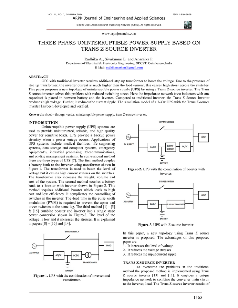
VOL. 11, NO. 2, JANUARY 2016
ARPN Journal of Engineering and Applied Sciences
ISSN 1819-6608
©2006-2016 Asian Research Publishing Network (ARPN). All rights reserved.
www.arpnjournals.com
THREE PHASE UNINTERRUPTIBLE POWER SUPPLY BASED ON
TRANS Z SOURCE INVERTER
Radhika A., Sivakumar L. and Anamika P.
Department of Electrical & Electronics Engineering, SKCET, Coimbatore, India
E-Mail: radhikamathan@gmail.com
ABSTRACT
UPS with traditional inverter requires additional step up transformer to boost the voltage. Due to the presence of
step up transformer, the inverter current is much higher than the load current, this causes high stress across the switches.
This paper proposes a new topology of uninterruptible power supply (UPS) by using a Trans Z-source inverter. The Trans
Z source inverter solves this problem with reduced switching stress. Here the impedance network (two inductors with one
capacitor) is placed in between battery and the inverter. Compared to traditional inverter, the Trans Z Source Inverter
produces high voltage. Further, it reduces the current ripple. The simulation model of a 3-Kw UPS with the Trans Z-source
inverter has been developed and verified.
Keywords: shoot – through vector, uninterruptible power supply, trans Z-source inverter.
INTRODUCTION
Uninterruptible power supply (UPS) systems are
used to provide uninterrupted, reliable, and high quality
power for sensitive loads. UPS provide a backup power
circuitry when a power outage occurs. Applications of
UPS systems include medical facilities, life supporting
systems, data storage and computer systems, emergency
equipment’s, industrial processing, telecommunications,
and on-line management systems. In conventional method
there are three types of UPS [7]. The first method couples
a battery bank to the inverter using transformer shown in
Figure-1. The transformer is used to boost the level of
voltage but it causes high current stresses on the switches.
The transformer also increases the weight, volume and
cost of the system. The second method couples a battery
bank to a booster with inverter shown in Figure-2. This
method requires additional booster which leads to high
cost and low efficiency. It complicates the controlling of
switches in the inverter. The dead time in the pulse width
modulation (PWM) is required to prevent the upper and
lower switches at the same leg. The third method [1] - [5]
& [15] combine booster and inverter into a single stage
power conversion shown in Figure-3. The level of the
voltage is low and it increases the stresses. It is explained
in papers [8] – [10] and [14].
Figure-2. UPS with the combination of booster with
inverter.
Figure-3. UPS with Z source inverter.
In this paper, a new topology using Trans Z source
inverter is proposed. The advantages of this proposed
paper are:
1. It increases the level of voltage
2. It reduces the voltage stresses
3. It reduces the input current ripple
Figure-1. UPS with the combination of inverter and
transformer.
TRANS Z SOURCE INVERTER
To overcome the problems in the traditional
method the proposed method is implemented using Trans
Z source inverter [13] and [11]. It employs a unique
impedance network to combine the converter main circuit
to the inverter, load. The Trans Z source inverter consist of
1365
VOL. 11, NO. 2, JANUARY 2016
ARPN Journal of Engineering and Applied Sciences
ISSN 1819-6608
©2006-2016 Asian Research Publishing Network (ARPN). All rights reserved.
www.arpnjournals.com
an inductor L1 and L2 and capacitor C1 connected in Tshape is employed to couple the circuit with the inverter.
In case of power outage the battery bank supplies power to
the inverter. The inverter consist of Trans Z source
symmetrical network (L1 = L2 and C1) and inverter (S1 –
S6). When the shoot-through vectors are taken the load is
shorted by upper and lower switches on the same leg of
the inverter. The proposed UPS can boost the voltage by
using shoot-through vectors shown in Figure-4.
(8)
Where,
(9)
B is the boost factor. If the voltage across the inductor Ls
is ignored, the output peak voltage is
(10)
Figure-4. Proposed UPS with Trans Z source inverter.
The inductor (L1 and L2) have the same
inductance, the Trans Z source network becomes
symmetrical. From the symmetrical and equivalent circuit
in Figure-5 (a) the voltage equation can be derived as
Where V1m is the peak value of fundamental voltage of
the inverter and m is modulation index (m ≤ 1).
The selection of the boost factor and the
modulation index can obtain the desired ac output voltage
regardless of the battery bank voltage.
The transfer function of the inverter is given as,
(1)
The voltage equation of the non-shoot through
states are derived as,
(11)
(2)
Where T0/Ts=d is the shoot through duty period.
The high switching frequency fs = 1/Ts. The capacitor
voltage over one switching period is constant, which is
equal to average input voltage.
(3)
Substituting (2) into (3) yields
(4)
When the Z-source inverter is working in shootthrough states shown in Figure-5 (b) during time interval
T0, where T0 = Ts − T1, and Ts is the switching period,
the inverter can be considered as a short circuit.
The voltage equation of the Trans Z-source
inverter at shoot-through states are,
(5)
The average voltage of inductor L1 (or L2) over one
switching period in steady-state operation is zero
(6)
Or
(7)
Substituting (7) into (4) gives
Figure-5. Equivalent circuit of Trans Z source inverter a)
non shoot through b) shoot through.
1366
VOL. 11, NO. 2, JANUARY 2016
ARPN Journal of Engineering and Applied Sciences
ISSN 1819-6608
©2006-2016 Asian Research Publishing Network (ARPN). All rights reserved.
www.arpnjournals.com
CONTROL OF PROPOSED UPS WITH TRANS Z
SOURCE INVERTER
The control of inductor current iL in the inner
loop and the output voltage V0 in the outer loop shown in
Figure-6 and it is based on paper [6] and [7].
Figure-8. Block diagram of outer loop.
Figure-6. Control system of Trans Z source inverter for
the proposed UPS system.
Inner Loop
The current feed forward control of the inner loop
has eliminated the load current disturbance shown in
Figure-7.
(12)
Where iL is the current across the filter. iref is the
reference voltage obtained from the comparison of
voltage.
Figure-7. Block diagram of inner loop.
Shoot Through Zero Vector Control
The zero vectors can be controlled to boost the
capacitor voltage in the Trans Z-source network, which
maintain the desired level of the average input voltage of
the Trans Z-source inverter. When the battery bank
voltage drops, voltage across the capacitor of the Trans Zsource inverter also drops. Thus, the voltage difference
between the reference and the actual capacitor voltage is
sent to the PI controller which generates the shoot-through
zero vectors.
The shoot through zero vectors can be calculated
as,
(16)
where H is the height of carrier wave. B is the
width of carrier wave. H1 value is obtained by comparing
the voltage across the battery and the reference value.
SIMULATION RESULTS
The simulation model of a 3-Kw UPS with the
Trans Z-source inverter has been developed.
The voltage and current waveform across the load
of the proposed UPS are shown in Figure-9 and 10.
The DC link Voltage of Trans Z Source Inverter
is shown in Figure-11.
Outer Loop
The output voltage V0 is regarded as a disturbance to
the current inner loop. To smooth the output voltage, a
voltage feed forward control is adopted shown in Figure-8.
(13)
Where Kw is the transfer function of voltage feed
forward controller.
(14)
The voltage across the inductor Ls can be given as,
(15)
Figure-9. Voltage and current waveform across the load
of the proposed UPS-open loop.
1367
VOL. 11, NO. 2, JANUARY 2016
ARPN Journal of Engineering and Applied Sciences
ISSN 1819-6608
©2006-2016 Asian Research Publishing Network (ARPN). All rights reserved.
www.arpnjournals.com
developed in MATLAB Simulink software and the results
are verified.
ACKNOWLEDGEMENTS
The authors would like to thank the management
of Sri Krishna college of Engineering and Technology for
their encouragement and support.
REFERENCES
[1] F. Z. Peng, “Z-source inverter,” IEEE Trans. Ind.
Appl., vol. 39,pp. 504–510, Mar./Apr. 2003.
[2] F. Z. Peng, M. Shen, and Z. Qian, “Maximum boost
control of the Z-source inverter,” IEEE Trans. Power
Electron., vol. 20, pp. 833–838, Jul.2005.
Figure-10. Voltage and current waveform across the load
of the proposed UPS-closed loop.
[3] M. Shen, J. Wang, A. Joseph, F. Z. Peng, L. M.
Tolbert, and D. J. Adams,“Constant boost control of
the Z-source inverter to minimize current ripple and
voltage stress,” IEEE Trans. Ind. Appl., vol. 42, pp.
770–778, May/Jun. 2006.
[4] P. C. Loh, D. M. Vilathgamuwa, G. J. Gajanayake, Y.
R. Lim, and C. W. Teo, “Transient modeling and
analysis of pulse width modulated Z Source Inverter,”
IEEE Trans. Power Electron., vol. 22, pp. 498–507,
Mar. 2007.
Figure-11. DC link voltage of Trans Z source inverter.
Table-1. Comparison of theoretical and simulated values
in open loop.
[5] Y. Huang, M. S. Shen, F. Z. Peng, and J.Wang, “ZSource inverter for residential photovoltaic systems,”
IEEE Trans. Power Electron, vol.21, pp. 1776-1782,
Nov 2006.
[6] M. Shen, A. Joseph, J. Wang, F. Z. Peng, and D. J.
Adams, “Comparison of traditional inverters and Zsource inverter for fuel cell vehicles,” IEEE Trans.
Power Electron., vol. 22, pp. 1453–1463, Jul. 2007.
[7] Z. J. Zhou, X. Zhang, P. Xu, and W. X. Shen,
“Single-phase uninterruptible power supply based on
Z-source inverter,” IEEE Trans. Ind. Electron., vol.
55, pp. 2997–3004, Aug. 2008.
Table-1 shows the comparative results of Inverter
and Trans ZSI. This results show us the increment of
voltage with less size, cost, and weight.
CONCLUSIONS
The traditional Z Source inverter is well suited
only for low modulation index condition. However, for
high modulation index the stress across the switches are
high. To sort out this problem Trans Z Source inverter has
been introduced. In this paper a three phase
uninterruptible power supply using Trans Z source
inverter has been designed and simulated. A model for 3Kw UPS with the Trans Z-source inverter has been
[8] J. Anderson and F. Z. Peng, “Four quasi-Z-source
inverters,” in 2008 Proc. IEEE PESC, pp. 2743–2749.
[9] P. C. Loh, P. C. Tan, and F. Blaabjerg, “Three Level
AC-DC-AC Z- Source Converter using reduced
passive component count, ” IEEE Trans. Power
Electron., vol.24, pp 1671-1681, Jul.2009.
[10] A. H. Rajaei, M. Mohamadian, S. M. Dehghan, and
A. Yazdian, “Single phase induction motor drive
system using z-source inverter,” IET Elect.Power
Appl., vol. 4, pp. 17–25, Jan. 2010.
[11] M. Zhu, D. Li, P. C. Loh and F.Blaabjerg, “Tappedinductor Z-source inverters with enhanced voltage
1368
VOL. 11, NO. 2, JANUARY 2016
ARPN Journal of Engineering and Applied Sciences
ISSN 1819-6608
©2006-2016 Asian Research Publishing Network (ARPN). All rights reserved.
www.arpnjournals.com
boost inversion abilities,” in 2010 Proc. IEEE
Sustainable Energy Technologies (ICSET), pp. 1 – 6.
[12] S.Yang, F.Z.Peng, Q. Lei, R.Inoshita and Zhaoming
Qian., “Current-fed quasi-Z-source inverter with
voltage buck-boost and regeneration capability,”
IEEE Transactions on Industrial Applications, Vol.47,
no.2, pp.882-892, Mar/Apr.2011.
[13] W. Qian, F. Z. Peng, and H. Cha, “Trans-Z-source
inverters,” IEEE Trans. Power Electron., vol. 26, pp.
3453–3463, Dec. 2011.
[14] L. Huang, M. Zhang, L. Hang, W. Yao, and Z. Lu, “A
Family of Three-Switch Three-State Single-Phase ZSource Inverters,” IEEE Trans. Power Electron, vol.
28, pp.2317-2329, May.2013.
[15] A.Radhika and L.Sivakumar, “An overview on
impedance source inverter control methods, types and
performance,” International Journal of Applied
Engineering Research, vol.10, pp. 33215-33225,
Nov.2015.
1369
