Digital Temperature Sensor
with SST Interface
ADT7484/ADT7486
Preliminary Technical Data
FEATURES
GENERAL DESCRIPTION
1 on-chip temperature sensor
1 or 2 remote temperature sensors
Simple Serial Transport™ (SST™) interface Rev 1 compliant
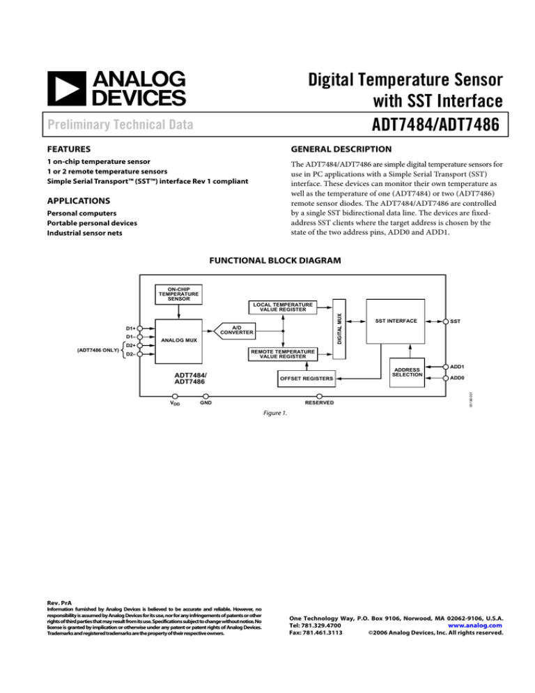
The ADT7484/ADT7486 are simple digital temperature sensors for
use in PC applications with a Simple Serial Transport (SST)
interface. These devices can monitor their own temperature as
well as the temperature of one (ADT7484) or two (ADT7486)
remote sensor diodes. The ADT7484/ADT7486 are controlled
by a single SST bidirectional data line. The devices are fixedaddress SST clients where the target address is chosen by the
state of the two address pins, ADD0 and ADD1.
APPLICATIONS
Personal computers
Portable personal devices
Industrial sensor nets
FUNCTIONAL BLOCK DIAGRAM
ON-CHIP
TEMPERATURE
SENSOR
A/D
CONVERTER
D1+
ANALOG MUX
D2+
(ADT7486 ONLY)
SST INTERFACE
SST
REMOTE TEMPERATURE
VALUE REGISTER
D2–
ADT7484/
ADT7486
VDD
OFFSET REGISTERS
GND
RESERVED
ADDRESS
SELECTION
ADD1
ADD0
05198-001
D1–
DIGITAL MUX
LOCAL TEMPERATURE
VALUE REGISTER
Figure 1.
Rev. PrA
Information furnished by Analog Devices is believed to be accurate and reliable. However, no
responsibility is assumed by Analog Devices for its use, nor for any infringements of patents or other
rights of third parties that may result from its use. Specifications subject to change without notice. No
license is granted by implication or otherwise under any patent or patent rights of Analog Devices.
Trademarks and registered trademarks are the property of their respective owners.
One Technology Way, P.O. Box 9106, Norwood, MA 02062-9106, U.S.A.
Tel: 781.329.4700
www.analog.com
Fax: 781.461.3113
©2006 Analog Devices, Inc. All rights reserved.
ADT7484/ADT7486
Preliminary Technical Data
TABLE OF CONTENTS
Features .............................................................................................. 1
SST Interface ..................................................................................8
Applications....................................................................................... 1
Temperature Measurement ........................................................... 11
General Description ......................................................................... 1
Temperature Measurement Method ........................................ 11
Functional Block Diagram .............................................................. 1
Reading Temperature Measurements...................................... 11
Revision History ............................................................................... 2
SST Temperature Sensor Data Format .................................... 12
Specifications..................................................................................... 3
Using Discrete Transistors ........................................................ 12
Absolute Maximum Ratings............................................................ 4
Layout Considerations............................................................... 12
Thermal Resistance ...................................................................... 4
Temperature Offset .................................................................... 13
ESD Caution.................................................................................. 4
Application Schematics ............................................................. 13
Pin Configurations And Functional Descriptions ....................... 5
Outline Dimensions ....................................................................... 14
Typical Performance Characteristics ............................................. 6
Ordering Guide .......................................................................... 14
Product Description ......................................................................... 8
REVISION HISTORY
4/06—Revision PrA: Preliminary Version
Rev. PrA | Page 2 of 16
Preliminary Technical Data
ADT7484/ADT7486
SPECIFICATIONS
TA = TMIN to TMAX, VCC = VMIN to VMAX, unless otherwise noted.
Table 1.
Parameter
POWER SUPPLY
Supply Voltage, VCC
Undervoltage Lockout Threshold
Average Operating Supply Current, IDD
TEMPERATURE-TO-DIGITAL CONVERTER
Local Sensor Accuracy
Min
Typ
Max
Unit
Test Conditions/Comments
3.0
3.3
2.8
1.4
3.6
V
V
mA
Continuous conversions
Remote Sensor Accuracy
Remote Sensor Source Current
Resolution
Conversion Time (Local Temperature)1
Conversion Time (Remote Temperature)1
Total Monitoring Cycle Time1
DIGITAL INPUTS (ADD0, ADD1)
Input High Voltage, VIH
Input Low Voltage, VIL
Input High Current, IIH
Input Low Current, IIL
Pin Capacitance
DIGITAL I/O (SST Pin)
Input High Voltage , VIH
Input Low Voltage, VIL
Hysteresis1
Output High Voltage, VOH
High Impedance State Leakage, ILEAK
SST TIMING
Bitwise Period, tBIT
High Level Time for Logic 1, tH1 2
High Level Time for Logic 0, tH0 2
Time to Assert SST High for Logic 1, tSU, HIGH
Hold Time, tHOLD3
Stop Time, tSTOP
Time to Respond After a Reset, tRESET
Response Time to Speed Negotiation
After Power-Up
°C
°C
°C
±3
°C
μA
μA
μA
°C
ms
ms
ms
6
36
96
0.016
12
38
50
2.1
0.8
−1
1
5
1.1
1.9
±1
±10
µA
150
1.1
V
V
μA
μA
pF
V
V
mV
V
µA
0.4
High Impedance State Leakage, ILEAK
Signal Noise Immunity, VNOISE
±1
±3
±1
300
mV p-p
0.495
0.65 × tBIT
0.2 × tBIT
0.75 × tBIT
0.25 × tBIT
1.25 × tBIT
2 × tBIT
500
0.8 × tBIT
0.4 × tBIT
0.2 × tBIT
0.5 × tBIT-M
2 × tBIT
µs
µs
µs
µs
µs
µs
0.4
ms
µs
500
1
Guaranteed by design, not production tested.
Minimum and maximum bit times are relative to tBIT defined in the timing negotiation pulse.
3
Devices compatible with hold time specification as driven by SST originator.
2
Rev. PrA | Page 3 of 16
40 ≤ TA ≤ 70°C, VCC = 3.3 V
−40 ≤ TA ≤ +125°C
−40 ≤ TD ≤ +125°C; −40 ≤ TA ≤ 70°C,
VCC = 3.3 V
−40 ≤ TD ≤ +125°C; −40 ≤ TA ≤ +125°C
Low level
Mid level
High level
Averaging enabled
Averaging enabled
Averaging enabled
VIN = VCC
VIN = 0
Between input switching levels
ISOURCE = 6 mA (maximum)
Device powered on SST bus;
VSST = 1.1 V, VCC = 3.3 V
Device unpowered on SST bus;
VSST = 1.1 V, VCC = 0 V
Noise glitches from 10 MHz to 100 MHz;
width up to 50 ns
tBIT defined in speed negotiation
See SST Specification Rev 1.0
Device responding to a constant low
level driven by originator
Time after power-up when device can
participate in speed negotiation
ADT7484/ADT7486
Preliminary Technical Data
ABSOLUTE MAXIMUM RATINGS
Table 2.
Parameter
Supply Voltage (VCC)
Voltage on Any Other Pin (Including SST Pin)
Input Current at Any Pin
Package Input Current
Maximum Junction Temperature (TJ max)
Storage Temperature Range
Lead Temperature, Soldering
IR Peak Reflow Temperature
Lead Temperature (10 sec)
ESD Rating
Rating
3.6 V
3.6 V
±5 mA
±20 mA
150°C
−65°C to +150°C
Stresses above those listed under Absolute Maximum Ratings
may cause permanent damage to the device. This is a stress
rating only; functional operation of the device at these or any
other conditions above those indicated in the operational
section of this specification is not implied. Exposure to absolute
maximum rating conditions for extended periods may affect
device reliability.
THERMAL RESISTANCE
260°C
300°C
2000 V
θJA is specified for the worst-case conditions, that is, a device
soldered in a circuit board for surface-mount packages.
Table 3. Thermal Resistance
Package Type
8-Lead MSOP (ADT7484)
10-Lead MSOP (ADT7486)
θJA
206
206
ESD CAUTION
ESD (electrostatic discharge) sensitive device. Electrostatic charges as high as 4000 V readily accumulate on
the human body and test equipment and can discharge without detection. Although this product features
proprietary ESD protection circuitry, permanent damage may occur on devices subjected to high energy
electrostatic discharges. Therefore, proper ESD precautions are recommended to avoid performance
degradation or loss of functionality.
Rev. PrA | Page 4 of 16
θJC
44
44
Unit
°C/W
°C/W
Preliminary Technical Data
ADT7484/ADT7486
GND 2
D1+ 3
ADT7484
TOP VIEW
(Not to Scale)
D1– 4
8
SST
7
ADD0
6
RESERVED
5
ADD1
VCC 1
10
SST
GND 2
ADT7486
9
ADD0
D1+ 3
TOP VIEW
(Not to Scale)
8
RESERVED
7
ADD1
6
D2–
D1– 4
D2+ 5
Figure 2. ADT7484 8-Lead MSOP
Figure 3. ADT7486 10-Lead MSOP
Table 4. ADT7484 Pin Function Descriptions
Pin No.
1
2
3
4
5
6
7
10
Mnemonic
VCC
GND
D1+
D1−
ADD1
RESERVED
ADD0
SST
Type
Power supply
Ground
Analog input
Analog input
Digital input
Reserved
Digital input
Digital input/output
Description
3.3 V ± 10%.
Ground Pin.
Positive Connection to Remote Temperature Sensor.
Negative Connection to Remote Temperature Sensor.
SST Address Select.
Connect to Ground.
SST Address Select.
SST Bidirectional Data Line.
Table 5. ADT7486 Pin Function Descriptions
Pin No.
1
2
3
4
5
6
7
8
9
10
Mnemonic
VCC
GND
D1+
D1−
D2+
D2−
ADD1
RESERVED
ADD0
SST
Type
Power supply
Ground
Analog input
Analog input
Analog input
Analog input
Analog input
Analog input
Digital input
Digital input/output
Description
3.3 V ± 10%.
Ground Pin.
Positive Connection to Remote 1 Temperature Sensor.
Negative Connection to Remote 1 Temperature Sensor.
Positive Connection to Remote 2 Temperature Sensor.
Negative Connection to Remote 2 Temperature Sensor.
SST Address Select.
Connect to Ground.
SST Address Select.
SST Bidirectional Data Line.
Rev. PrA | Page 5 of 16
05198-003
VCC 1
05198-002
PIN CONFIGURATIONS AND FUNCTIONAL DESCRIPTIONS
ADT7484/ADT7486
Preliminary Technical Data
TYPICAL PERFORMANCE CHARACTERISTICS
Figure 4. SST O/P Level vs. Supply Voltage
Figure 7. SST O/P Level vs. Pull Down(?)
Figure 5. Supply Current vs. Temperature
Figure 8. Supply Current vs. Voltage
Figure 6. Local Temperature Error
Figure 9. Remote Temperature Error
Rev. PrA | Page 6 of 16
Preliminary Technical Data
ADT7484/ADT7486
Figure 10. Remote Temperature Error vs. PCB Resistance
Figure 13. Remote Temperature Error vs. Capacitance Between D1+ and D1−
Figure 11. Temperature Error vs. Common-Mode Noise Frequency
Figure 14. Temperature Error vs. Differential Mode Noise Frequency
Figure 12. Temperature Error vs. Power Supply Noise
Rev. PrA | Page 7 of 16
ADT7484/ADT7486
Preliminary Technical Data
PRODUCT DESCRIPTION
The ADT7484 is a single remote temperature sensor, and the
ADT7486 is a dual temperature sensor for use in PC applications.
The ADT7484/ADT7486 accurately measure local and remote
temperature and communicate over a one-wire Simple Serial
Transport (SST) bus interface.
SST INTERFACE
Simple Serial Transport (SST) is a one-wire serial bus and a
communications protocol between components intended for
use in personal computers, personal handheld devices, or other
industrial sensor nets. The ADT7484/ADT7486 support SST
specification Rev 1.
SST is a licensable bus technology from Analog Devices, Inc., and
Intel Corporation. To inquire about obtaining a copy of the Simple
Serial Transport Specification or an SST technology license,
please email Analog Devices, Inc., at sst_licensing@analog.com
or write to Analog Devices, Inc., 3550 North First Street, San
Jose, CA 95134, Attention: SST Licensing, M/S B7-24.
ADT7486 Client Address
The client address for the ADT7484/ADT7486 is selected using
the address pin. The address pin is connected to a float
detection circuit, which allows the ADT7484/ADT7486 to
distinguish between three input states: high, low (GND), and
floating. The address range for fixed address, discoverable
devices is 0x48 to 0x50.
Table 6. ADT7484/ADT7486 Selectable Addresses
ADD1
Low (GND)
Low (GND)
Low (GND)
Float
Float
Float
High
High
High
Rev. PrA | Page 8 of 16
ADD0
Low (GND)
Float
High
Low (GND)
Float
High
Low (GND)
Float
High
Address Selected
0x48
0x49
0x4A
0x4B
0x4C
0x4D
0x4E
0x4F
0x50
Preliminary Technical Data
ADT7484/ADT7486
Command Summary
Table 7 summarizes the commands supported by the ADT7484/ADT7486 devices when directed at the target address selected by the fixed
address pins. It contains the command name, command code (CC), write data length (WL), read data length (RL), and a brief description.
Table 7. Command Code Summary
Command
Ping()
Command Code, CC
0x00
Write Length, WL
0x00
Read Length, RL
0x00
Description
Shows a nonzero FCS over the header if present.
GetIntTemp()
0x00
0x01
0x02
GetExt1Temp()
0x01
0x01
0x02
Shows the temperature of the device’s internal
thermal diode.
Shows the temperature of External Thermal Diode 1.
GetExt2Temp()
0x02
0x01
0x02
GetAllTemps()
0x00
0x01
0x04 (ADT7484)
0x06 (ADT7486)
SetExt1Offset()
0xe0
0x03
0x00
GetExt1Offset()
0xe0
0x01
0x02
SetExt2Offset()
0xe1
0x03
0x00
GetExt2Offset()
0xe1
0x01
0x02
ResetDevice()
0xf6
0x01
0x00
GetDIB()
0xf7
0xf7
0x01
0x01
0x08
0x10
Rev. PrA | Page 9 of 16
Shows the temperature of External Thermal Diode 2
(ADT7486 only).
Shows a 4- or 6-byte block of data (ADT7484: GetIntTemp,
GetExt1Temp; ADT7486: GetIntTemp, GetExt1Temp,
GetExt2Temp).
Sets the offset used to correct errors in External Diode 1.
Shows the offset that the device is using to correct
errors in External Diode 1.
Sets the offset used to correct errors in External Diode 2
(ADT7486 only).
Shows the offset that the device is using to correct
errors in External Diode 2 (ADT7486 only).
Functional reset. The ADT7484/ADT7486 also respond to
this command when directed to the Target Address 0x00.
Shows information used by SW to identify the device’s
capabilities. Can be in 8- or 16-byte format.
ADT7484/ADT7486
Preliminary Technical Data
Command Code Details
ADT7484/ADT7486 Device Identifier Block
GetIntTemp()
The GetDIB() command retrieves the device identifier block
(DIB), which provides information to identify the capabilities of
the ADT7484/ADT7486. The data returned can be in 8- or 16byte format. The full 16 bytes of DIB is detailed in Table 8. The
8-byte format involves the first eight bytes described in this
table. Byte-sized data is returned in the respective fields as it
appears in Table 8. Word-sized data, including vendor ID,
device ID, and data values use little endian format, that is, the
LSB is returned first, followed by the MSB.
Table 8. DIB Byte Details
Value
0xc0
0x10
Vendor ID
00x11d4
Device ID
0x7484
or
0x7486
0x01
0x00
0x00
0x00
0x00
0x48 to
0x50
The ADT7484 shows the local and remote temperatures in a 4-byte
block of data (internal temperature first, followed by External
Temperature 1) in response to a GetAllTemps() command. The
ADT7486 shows the local and remote temperatures in a 6-byte
block of data (internal temperature first, followed by External
Temperature 1 and External Temperature 2) in response to this
command.
SST device
Reserved
Reserved
Reserved
Reserved
Dependent on the state of
the address pins.
This command sets the offset that the ADT7484/ADT7486 will
use to correct errors in the external diode. The offset is set in
little endian, 16-bit, twos compliment format. The maximum
offset is ±128°C with +0.25°C resolution.
The Ping() command verifies if a device is responding at a
particular address. The ADT7484/ADT7486 show a valid
nonzero FCS in response to the Ping() command when
correctly addressed.
Write Length
0x00
Read Length
0x00
FCS
ResetDevice()
This command resets the register map and conversion
controller. The reset command can be global or directed at the
client address of the ADT7484/ADT7486.
Table 10. ResetDevice() Command
Write
Length
0x01
Read
Length
0x00
Reset
command
0xf6
SetExtOffset()
GetExtOffset()
This command causes the ADT7484/ADT7486 to show the
offset that they are using to correct errors in the external diode.
The offset value is returned in little endian format, that is, LSB
before MSB.
ADT7484/ADT7486 Response to Unsupported Commands
Table 9. Ping() Command
Target Address
Device Address
Prompted by the GetExtTemp() command, the
ADT7484/ADT7486 show the temperature of the remote diode
in little endian, 16-bit, twos compliment format. The
ADT7484/ADT7486 show 0x8000 in response to this command
if the external diode is an open or short circuit.
Description
Fixed address device.
Meets Version 1 of the SST
specification
Contains company ID
number in little endian
format
Contains device ID number
in little endian format
Ping()
Target Address
Device Address
GetExtTemp()
GetAllTemps()
Name
Device Capabilities
Version/Revision
Device Interface
Function Interface
Reserved
Reserved
Vendor Specific ID
Client Device Address
The ADT7484/ADT7486 show the local temperature of the
device in response to the GetIntTemp() command. The data has
a little endian, 16-bit, twos compliment format.
A full list of command codes supported by the ADT7484/
ADT7486 is given in Table 7. The offset registers (Command
Codes 0xe0 and 0xe1) are the only registers that the user can
write to. The other defined registers are read only. Writing to
Register Addresses 0x03 to 0xdf shows a valid FSC, but no
action is taken by the ADT7484/ADT7486. The
ADT7484/ADT7486 show an invalid FSC if the user attempts to
write to the devices between Command Codes 0xe2 to 0xee and
no data is written to the device. These registers are reserved for
the manufacturer’s use only, and no data can be written to the
device via these addresses.
FCS
Rev. PrA | Page 10 of 16
Preliminary Technical Data
ADT7484/ADT7486
TEMPERATURE MEASUREMENT
The ADT7484/ADT7486 each have two dedicated temperature
measurement channels: one for measuring the temperature of an
on-chip band gap temperature sensor, and one for measuring the
temperature of a remote diode, usually located in the CPU or GPU.
The ADT7484 monitors one local and one remote temperature
channel, whereas the ADT7486 monitors one local and two
remote temperature channels. Monitoring of each of the
channels is done in a round-robin sequence. The monitoring
sequence is in the order shown in Table 11.
Table 11. Temperature Monitoring Sequence
Channel
Number
0
1
2
Measurement
Local temperature
Remote Temperature 1
Remote Temperature 2
(ADT7486 only)
Conversion Time (ms)
52
52
52
To measure ΔVBE, the operating current through the sensor is
switched between three related currents. Figure 15 shows N1 × I
and N2 × I as different multiples of the current I. The currents
through the temperature diode are switched between I and
N1 × I, giving ΔVBE1, and then between I and N2 × I, giving
ΔVBE2. The temperature can then be calculated using the two
ΔVBE measurements. This method can also cancel the effect of
series resistance on the temperature measurement. The
resulting ΔVBE waveforms are passed through a 65 kHz low-pass
filter to remove noise and then through a chopper-stabilized
amplifier to amplify and rectify the waveform, producing a dc
voltage proportional to ΔVBE. The ADC digitizes this voltage,
and a temperature measurement is produced. To reduce the
effects of noise, digital filtering is performed by averaging the
results of 16 measurement cycles for low conversion rates.
Signal conditioning and measurement of the internal
temperature sensor is performed in the same manner.
VDD
I
A simple method for measuring temperature is to exploit the
negative temperature coefficient of a diode by measuring the
base-emitter voltage (VBE) of a transistor operated at constant
current. Unfortunately, this technique requires calibration to
null the effect of the absolute value of VBE, which varies from
device to device.
The technique used in the ADT7484/ADT7486 measures the
change in VBE when the device is operated at three different
currents.
Figure 15 shows the input signal conditioning used to measure
the output of a remote temperature sensor. This figure shows
the remote sensor as a substrate transistor, which is provided for
temperature monitoring on some microprocessors, but it could
also be a discrete transistor. If a discrete transistor is used, the
collector is not grounded and should be linked to the base. To
prevent ground noise from interfering with the measurement,
the more negative terminal of the sensor is not referenced to
ground, but is biased above ground by an internal diode at the
D1− input. If the sensor is operating in an extremely noisy
environment, C1 can be added as a noise filter. Its value should
not exceed 1000 pF.
REMOTE
SENSING
TRANSISTOR
N1 × I
N2 × I
IBIAS
D+
VOUT+
C1*
TO ADC
D–
BIAS
DIODE
VOUT–
LOW-PASS FILTER
fC = 65kHz
*CAPACITOR C1 IS OPTIONAL. IT SHOULD ONLY BE USED IN NOISY ENVIRONMENTS.
05198-004
TEMPERATURE MEASUREMENT METHOD
Figure 15. Signal Conditioning for Remote Diode Temperature Sensors
READING TEMPERATURE MEASUREMENTS
The temperature measurement command codes are detailed in
Table 10. The temperature data returned is two bytes in little
endian format, that is, LSB before MSB. All temperatures can be
read together by using Command Code 0x00 with a read length
of 0x04. The command codes and returned data are described
in Table 12.
Table 12. Temperature Channel Command Codes
Temp Channel
Internal
External 1
External 2
All Temps
Rev. PrA | Page 11 of 16
Command Code
0x00
0x01
0x02
0x00
Returned data
LSB, MSB
LSB, MSB
LSB, MSB
Internal LSB, Internal MSB;
External 1 LSB, External 1
MSB; External 2 LSB,
External 2 MSB
ADT7484/ADT7486
Preliminary Technical Data
SST TEMPERATURE SENSOR DATA FORMAT
LAYOUT CONSIDERATIONS
The data for temperature is structured to allow values in the
range of ±512°C to be reported. Thus, the temperature sensor
format uses a twos complement, 16-bit binary value to represent
values in this range. This format allows temperatures to be
represented with approximately a 0.016°C resolution.
Digital boards can be electrically noisy environments. Take the
following precautions to protect the analog inputs from noise,
particularly when measuring the very small voltages from a
remote diode sensor:
•
Table 13. SST Temperature Data Format
Twos Compliment
MSB
LSB
1110 0000
1100 0000
1110 1100
0000 0000
1111 0110
0000 0000
1111 1011
0011 1110
1111 1110
1100 0000
1111 1111
1100 0000
0000 0000
0000 0000
0000 0000
0100 0000
0000 0001
0100 0000
0000 0100
1100 0010
0000 1010
0000 0000
0001 0100
0000 0000
0001 1111
0100 0000
•
•
5MIL
GND
5MIL
D+
5MIL
5MIL
5MIL
D–
5MIL
GND
USING DISCRETE TRANSISTORS
If a discrete transistor is used, the collector is not grounded and
should be linked to the base. If a PNP transistor is used, the
base is connected to the D1− input and the emitter is connected
to the D1+ input. If an NPN transistor is used, the emitter is
connected to the D1− input and the base is connected to the
D1+ input. Figure 15 shows how to connect the
ADT7484/ADT7486 to an NPN or PNP transistor for
temperature measurement. To prevent ground noise from
interfering with the measurement, the more negative terminal
of the sensor is not referenced to ground, but is biased above
ground by an internal diode at the D1− input.
D+
D–
ADT7484/
ADT7486
D+
2N3906
PNP
•
•
•
•
ADT7484/
ADT7486
D–
Figure 17. Arrangements of Signal Tracks
05198-005
2N3904
NPN
•
Figure 16. Connections for NPN and PNP Transistors
The ADT7484/ADT7486 show an external temperature value of
0x8000 if the external diode is an open or short circuit.
5MIL
05198-006
Temperature (°C)
−125
−80
−40
−20
−5
−1
0
+1
+5
+20
+40
+80
+125
Place the device as close as possible to the remote sensing
diode. Provided that the worst noise sources, such as clock
generators, data/address buses, and CRTs, are avoided, this
distance can be four to eight inches.
Route the D1+ and D1− tracks close together in parallel
with grounded guard tracks on each side. Provide a ground
plane under the tracks if possible.
Use wide tracks to minimize inductance and reduce noise
pickup. A 5 mil track minimum width and spacing is
recommended.
Try to minimize the number of copper/solder joints, which
can cause thermocouple effects. Where copper/solder
joints are used, make sure that they are in both the D1+
and D1− paths and are at the same temperature.
Thermocouple effects should not be a major problem because
1°C corresponds to about 240 µV, and thermocouple voltages
are about 3 µV/°C of the temperature difference. Unless there
are two thermocouples with a big temperature differential
between them, thermocouple voltages should be much less
than 200 mV.
Place a 0.1 µF bypass capacitor close to the device.
If the distance to the remote sensor is more than eight
inches, the use of a twisted-pair cable is recommended.
This works for distances of about six to 12 feet.
For very long distances (up to 100 feet), use shielded twistedpair cables, such as Belden #8451 microphone cables.
Connect the twisted-pair cable to D1+ and D1− and the
shield to GND, close to the device. Leave the remote end of
the shield unconnected to avoid ground loops.
Because the measurement technique uses switched current
sources, excessive cable and/or filter capacitance can affect the
measurement. When using long cables, the filter capacitor can
be reduced or removed. Cable resistance can also introduce
errors. A 1 Ω series resistance introduces about 0.5°C error.
Rev. PrA | Page 12 of 16
Preliminary Technical Data
ADT7484/ADT7486
APPLICATION SCHEMATICS
VCC
2N3904 OR CPU
THERMAL DIODE
Rev. PrA | Page 13 of 16
ADT7484
1
VCC
SST
8
2
GND
ADD0
7
3
D1+ RESERVED
6
4
D1–
5
ADD1
SST
05198-007
As CPUs run faster, it is more difficult to avoid high frequency
clocks when routing the D1+ and D1− tracks around a system
board. Even when the recommended layout guidelines are
followed, there may still be temperature errors, attributed to
noise being coupled on to the D1+ and D1− lines. High
frequency noise generally has the effect of producing
temperature measurements that are consistently too high by a
specific amount. The ADT7484/ADT7486 have a temperature
offset command code of 0xe0 through which a desired offset
can be set. By doing a one-time calibration of the system, the
offset caused by system board noise can be calculated and
nulled by specifying it in the ADT7484/ADT7486. The offset is
automatically added to every temperature measurement. The
maximum offset is ±128°C with 0.25°C resolution. The offset
format is the same as the temperature data format—16-bit, twos
compliment notation, as shown in Table 13. The offset should
be programmed in little endian format, that is, LSB before MSB.
The offset value is also returned in little endian format when read.
Figure 18. ADT7484 Typical Application Schematic
VCC
2N3904
NPN
ADT7486
1
VCC
2
GND
ADD0
SST 10
9
3
D1+ RESERVED
8
4
D1–
ADD1
7
5
D2+
D2–
6
SST
CPU
THERMAL
DIODE
Figure 19. ADT7486 Typical Application Schematic
05198-008
TEMPERATURE OFFSET
ADT7484/ADT7486
Preliminary Technical Data
OUTLINE DIMENSIONS
Figure 20. 8-Lead Mini Small Outline Package [MSOP]
(RM-8)
Dimensions shown in millimeters
3.10
3.00
2.90
10
3.10
3.00
2.90
1
6
5.15
4.90
4.65
5
PIN 1
0.50 BSC
0.95
0.85
0.75
0.15
0.05
1.10 MAX
0.33
0.17
SEATING
PLANE
0.23
0.08
8°
0°
0.80
0.60
0.40
COPLANARITY
0.10
COMPLIANT TO JEDEC STANDARDS MO-187-BA
Figure 21. 10-Lead Mini Small Outline Package [MSOP]
(RM-10)
Dimensions shown in millimeters
ORDERING GUIDE
Model
ADT7484ARMZ1
ADT7484ARMZ-REEL1
ADT7484ARMZ-REEL71
ADT7486ARMZ1
ADT7486ARMZ-REEL1
ADT7486ARMZ-REEL71
1
Temperature Range
–40°C to +125°C
–40°C to +125°C
–40°C to +125°C
–40°C to +125°C
–40°C to +125°C
–40°C to +125°C
Package Description
8-Lead MSOP
8-Lead MSOP
8-Lead MSOP
10-Lead MSOP
10-Lead MSOP
10-Lead MSOP
Z = Pb-free part.
Rev. PrA | Page 14 of 16
Package Option
RM-8
RM-8
RM-8
RM-10
RM-10
RM-10
Preliminary Technical Data
ADT7484/ADT7486
NOTES
Rev. PrA | Page 15 of 16
ADT7484/ADT7486
Preliminary Technical Data
NOTES
©2006 Analog Devices, Inc. All rights reserved. Trademarks and
registered trademarks are the property of their respective owners.
PR05198-0-4/06(PrA)
Rev. PrA | Page 16 of 16
