0.25 μm CMOS Process
FC025
MIXED-SIGNAL FOUNDRY EXPERTS
0.25 Micron CMOS Technology
Description
Key Features
Applications
Quality
Assurance
Deliverables
Digital
Libraries
Analog
Libraries
Primitive
Devices
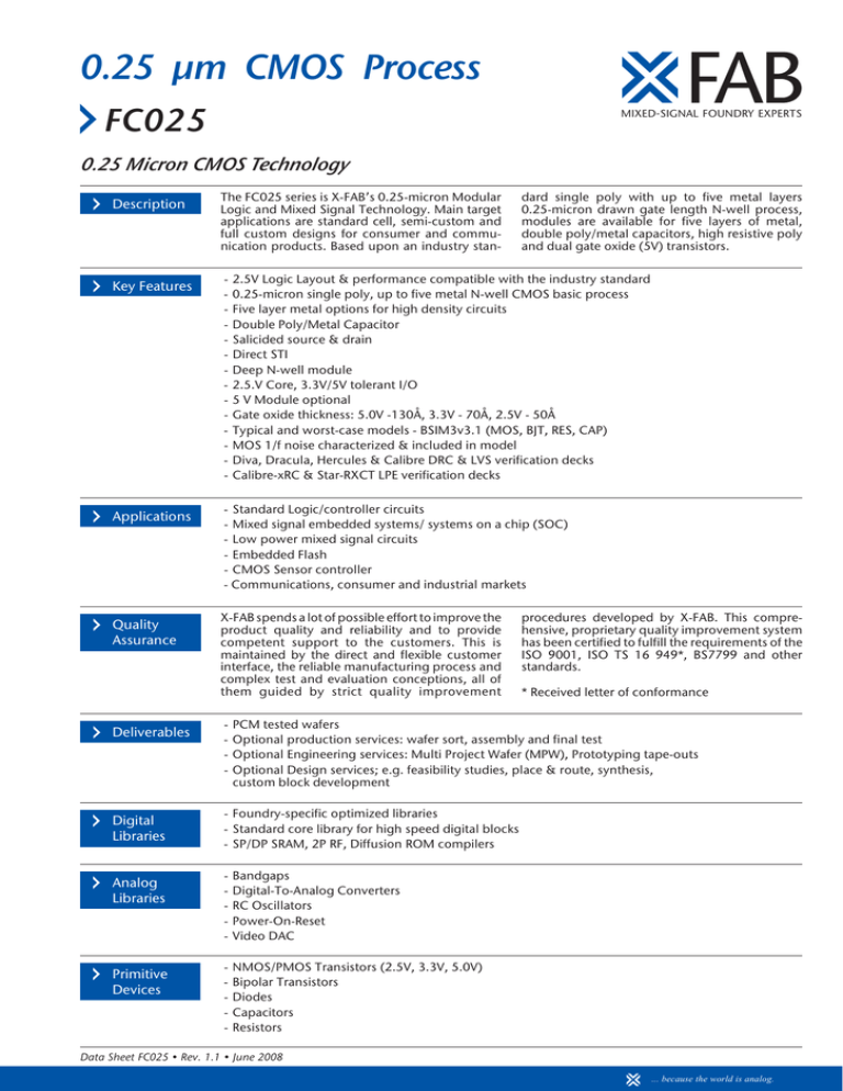
The FC025 series is X-FAB’s 0.25-micron Modular
Logic and Mixed Signal Technology. Main target
applications are standard cell, semi-custom and
full custom designs for consumer and communication products. Based upon an industry stan-
dard single poly with up to five metal layers
0.25-micron drawn gate length N-well process,
modules are available for five layers of metal,
double poly/metal capacitors, high resistive poly
and dual gate oxide (5V) transistors.
2.5V Logic Layout & performance compatible with the industry standard
0.25-micron single poly, up to five metal N-well CMOS basic process
Five layer metal options for high density circuits
Double Poly/Metal Capacitor
Salicided source & drain
Direct STI
Deep N-well module
2.5.V Core, 3.3V/5V tolerant I/O
5 V Module optional
Gate oxide thickness: 5.0V -130Å, 3.3V - 70Å, 2.5V - 50Å
Typical and worst-case models - BSIM3v3.1 (MOS, BJT, RES, CAP)
MOS 1/f noise characterized & included in model
Diva, Dracula, Hercules & Calibre DRC & LVS verification decks
Calibre-xRC & Star-RXCT LPE verification decks
- Standard Logic/controller circuits
- Mixed signal embedded systems/ systems on a chip (SOC)
- Low power mixed signal circuits
- Embedded Flash
- CMOS Sensor controller
- Communications, consumer and industrial markets
X-FAB spends a lot of possible effort to improve the
product quality and reliability and to provide
competent support to the customers. This is
maintained by the direct and flexible customer
interface, the reliable manufacturing process and
complex test and evaluation conceptions, all of
them guided by strict quality improvement
-
procedures developed by X-FAB. This comprehensive, proprietary quality improvement system
has been certified to fulfill the requirements of the
ISO 9001, ISO TS 16 949*, BS7799 and other
standards.
* Received letter of conformance
PCM tested wafers
Optional production services: wafer sort, assembly and final test
Optional Engineering services: Multi Project Wafer (MPW), Prototyping tape-outs
Optional Design services; e.g. feasibility studies, place & route, synthesis,
custom block development
- Foundry-specific optimized libraries
- Standard core library for high speed digital blocks
- SP/DP SRAM, 2P RF, Diffusion ROM compilers
-
Bandgaps
Digital-To-Analog Converters
RC Oscillators
Power-On-Reset
Video DAC
-
NMOS/PMOS Transistors (2.5V, 3.3V, 5.0V)
Bipolar Transistors
Diodes
Capacitors
Resistors
Data Sheet FC025 • Rev. 1.1 • June 2008
... because the world is analog.
FC025
Process Options
Module Name
Number of Masks
Remarks
Typical Primitive Devices Applications
CMOS Core (1P3M)
17
P-prime wafer, single poly, triple metal
2.5V/3.3V NMOS/PMOS, digital applications
To get the available technology options; this main module can be combined with one or more of the following additional modules:
Module Name
Number of
additional Masks
Remarks
Typical Primitive Devices Applications
PIP
2
Double polysilicon process
Capacitor
MIM
1
Metal-insulator-Metal process
Capacitor
HRPOLY
1
LPP mask
High value resistor
5 Volt
2
RACT & NW2 masks
5 Volt NMOS & 5 Volt PMOS transistors
Deep Nwell
2
Deep Nwell implantation
Noise isolation
SRAM
1
7.56μm² SRAM process
SRAM bit cell
Metal 4
2
Additional Metal layer
More complex wiring
Metal 5
2
Additional Metal layer
More complex wiring
Module Name
Number of Masks
Remarks
Typical Primitive Devices Applications
eFlash (2P3M)
32
P-prime wafer, double poly,
logic with mixed signal, embedded Flash
2.5V/3.3V NMOS/PMOS, Smart card / MCU
Schematic Cross Sections
Pad
Nitride
Pad
Oxide
MTP (top Metal)
VIA (top Via)
Metal
CM (top plate)
BM (bottom plate)
NH
STI
PMOS
PMOS
NM
Figure 1:
Process Section
(Via)
Where N can be
1st, 2nd, 3rd and 4th.
Figure 2:
Page 2
MIM Module
(Metal)
FC025
Alignment
ALIGN KEY
deep N-well
DNWELL
5V NMOS transistor
implant
5V
NDD
SRAM
Lightly P+ Poly
implant
HIGH RS POLY
ESD implant layer
ESD
PIP / MIM Deposition
CAPACITOR
Active area
P-well
N-well
Gate Poly
Active
Poly
Area
2.5V NMOS transistor
implant
3.3V NMOS transistor or
implant
2.5V PMOS transistor
implant
N+ implant
P+ implant
Salicide Deposition
Contact
Metal 1
Via 1
Metal 2
Via 2
Metal 3
Via 3
Metal 4
Via L
Thick Metal 5
METAL3
THKMET
Additional Modules
CMOS Module
Main Process Flow
Pads
Back side grinding
(on customer request)
mask steps
Page 3
FC025
Basic Design Rules
Mask
Width [μm]
Spacing [μm]
N-Well
1.2
2.0
Active Area
0.3
0.4
Poly-Silicon Gate
0.24
0.4
Contact
0.3
0.3
Metal 1
0.32
0.32
Via 1
0.36
0.35
Metal 2
0.4
0.4
Via 2
0.36
0.35
Metal 3
0.4
0.4
Via 3
0.36
0.35
Metal 4
0.4
0.4
VTP
0.36
0.35
MTP
0.44
0.46
Device Parameters
Active Devices (typical data)
MOS Transistors
Device
Available with
module
|VT|
[V]
IDS
[μA/μm]
|BVDSS|
[V]
NMOS 2.5V
core
0.53
600
> 5
PMOS 2.5V
core
-0.53
-270
< -5
NMOS 3.3V
3.3V I/O
0.53
580
> 6
PMOS 3.3V
3.3V I/O
-0.83
-230
< -6
NMOS 5V
5V I/O
0.83
530
> 7
PMOS 5V
5V I/O
0.82
-240
< -7
Device
Area Cap
[fF/μm2]
BV
[V]
Voltage coefficient
[ppm/V]
Poly1-Poly2
0.9
>10
200
Metal-insulator-Metal
1.0
>10
100
Passive Devices (typical data)
Capacitors
Page 4
FC025
Device Parameters (continued)
Passive Devices (typical data) (continued)
Resistors & Conductors
Device
RS
[Ω/
]
Thickness
[μm]
Max J/W
[mA/μm]
N+ Poly resistor (salicide)
5
0.20
-
P+ Poly resistor (salicide)
5
0.20
-
N+ Poly resistor (non-salicide)
190
0.16
-
P+ Poly resistor (non-salicide)
160
0.16
-
P+ Poly resistor high Rs (non-salicide)
900
0.16
-
P+ Poly resistor medium Rs (non-salicide)
500
0.16
-
P+ diffusion silicided resistor
4.0
0.22
-
P+ diffusion resistor
140
0.17
-
N+ diffusion silicided resistor
4.5
0.20
-
N+ diffusion resistor
65
0.15
-
N-well resistor
1100
1.5
-
Deep N-well resistor
500
-
-
Metal 1
0.08
0.44
1
Metal 2
0.06
0.44
1
Metal 3
0.06
0.44
1
Metal 4
0.06
0.44
1
Metal 5 (top metal)
0.04
0.85
1.6
Digital Core
Cells Cells
Library
ARM Standard cells up to 70K gates/mm2
6T SRAM Cell: 7.56μm2 & 10.95μm2
Memory Compilers:
- ARM – SP & DP SRAM Compiler
- ARM – 2P RF Compilers
- ARM – Diffusion ROM Compiler
eFlash Macro
Digital
I/O Cells
IP Macro
Configuration
AF16K8AF25
16K x 8
AF32K8AF25
32K x 8
AF32K8BF25
32K x 8
AF64K8AF25
64K x 8
AF64K8BF25
64K x 8
AF128K8GF25
128K x 8
AF256K8CF25
256K x 8
AF256K16FF25
256K x 16
The digital I/O library contains a comprehensive
range of I/O cells divided into distinct inputs,
outputs and bidirectionals with variants for single
voltage and dual voltage devices.
The digital I/O library has the following features:
- ARM – Integral I/O (90um pitch)
- ARM – GPIO (60um pitch)
- ARM – USB 1.1 IO
- ARM – 5V tolerant I/O cells are available.
Page 5
FC025
Logic &
Mixed Signal
Primitive
Devices and
Models
See section “Device Parameters” for details.
X-FAB’s CAE support kit Cadence PDK.
X-FAB supports BSIM3 models as the present SPICE
model standard for MOS transistors. Well resistors
have a non-linear terminal-voltage and bulkvoltage dependence. These resistances have to be
simulated with the 3-terminal SPICE JFET model.
Model sets for most popular analog simulators,
e.g. Spectre, HSPICE and PSPICE are provided.
Examples for measured and modeled parameter characteristics
CMOS and Bipolar Transistor Output Characteristics
Figure 3:
2.5V NMOS Output Characteristic
Figure 3:
2.5V PMOS Output Characteristic
Figure 5:
3.3V NMOS Output Characteristic
Figure 6:
3.3V PMOS Output Characteristic
Figure 7:
2.5V Native NMOS
Figure 8:
3.3V Native NMOS
Page 6
FC025
Examples for measured and modeled parameter characteristics (continued)
2.5V BJT (Emitter size 2x2 μm²) Gummel Plot
Figure 10: Gain vs collector current
Figure 11: 3.3V BJT (Emitter size 2x2 μm²) Gummel Plot
Figure 12: Gain vs collector current
Figure 9:
Matching
Figure 13: 2.5V NMOS Vt Matching
Figure 15: 3.3V NMOS Vt Matching
Figure 14: 2.5V PMOS Vt Matching
Figure 16: 3.3V PMOS Vt Matching
Page 7
FC025
Examples for measured and modeled parameter characteristics (continued)
Resistor Matching
Figure 17: N+ Poly Resistance Matching
Figure 18: P+ Poly Resistance Matching
Figure 19: N+ Poly (non-salicide) Resistance Matching
Figure 20: P+ Poly (non-salicide) Resistance Matching
Mixed Signal
Library Cells
Many logic and mixed-signal design projects are
started in old technologies because designers want
to re-use existing analog cells. For easy migration
Page 8
to X-FAB’s high performance FC025 process an
increasing number of general purpose analog cells
will be provided.
FC025
Supported CAE Service / Tools
Frontend Design Environment
Synthesis
Digital
Simulation
Timing,
Power,
Signal-Integrity
Analysis
Mixed-SignalSimulators
Analog
Simulators
Mixed Signal Environment
Floorplanning, Place & Route
Layout / Chip assembly drawing
Verification & SignOff
Tape Out / GDSII
Note: Diagram shows overview of reference flow at X-FAB. Detailed information of supported EDA tools for major vendors like
Cadence, Mentor and Synopsys can be found on X-FAB's online technical information center, X-TIC.
0.25μm Process
Mentor
Synopsys
Cadence
Foundry process (F)
Calibre DRC/LVS
Calibre xRC
Hercules DRC/LVS
Star-RCXT
Techfile
Foundry Compatible process (FC)
Calibre DRC/LVS
Calibre xRC
Hercules DRC/LVS
Star-RCXT
Techfile / Diva DRC/LVS
Dracula DRC/LVS/LPE
eFlash process (eFlash)
Calibre DRC/LVS
Calibre xRC
Hercules DRC/LVS
Star-RCXT
Techfile / Diva DRC/LVS
Dracula DRC/LVS/LPE
Addresses
Quality Data
Important
Notice
Marketing & Sales Headquarters
X-FAB Semiconductor Foundries AG
Haarbergstr. 67, 99097 Erfurt, Germany
Tel.:
+49-361-427 6160
Fax:
+49-361-427 6161
Email: Thomas.Hartung@xfab.com
Web: http://www.xfab.com
Quality Data are available on request. Contact:
Information
info@xfab.com
Technology & Design Support
hotline@xfab.com
Silicon Foundry Services
sifo@xfab.com
X-FAB Semiconductor Foundries AG
Quality Assurance
Haarbergstr. 67
99097 Erfurt, Germany
Products sold by X-FAB are covered by the warranty provisions appearing in its Term of Sale. X-FAB makes no warranty, express,
statutory, implied, or by description regarding the information set forth herein or regarding the freedom of the described devices
from patent infringement. X-FAB reserves the right to change specifications and prices at any time and without notice. Therefore,
prior to designing this product into a system, it is necessary to check with X-FAB for current information. This product is intended
for use in normal commercial applications. Applications requiring extended temperature range, unusual environmental requirements,
or high reliability applications, such as medical life-support or life-sustaining equipment are specifically not recommended without
additional processing by X-FAB for each application.
The information furnished by X-FAB is believed to be correct and accurate. However, X-FAB shall not be liable to recipient or any third
party for any damages, including but not limited to personal injury, property damage, loss of profits, loss of use, interrupt of business
or indirect, special incidental or consequential damages, of any kind, in connection with or arising out of the furnishing, performance
or use of the technical data herein. No obligation or liability to recipient or any third party shall arise or flow out of X-FAB’s rendering
of technical or other services.
© 1999-2008 by X-FAB Semiconductor Foundries AG. All rights reserved.
Page 9
