Design of Ripple Borrow Subtractor using different logic
advertisement

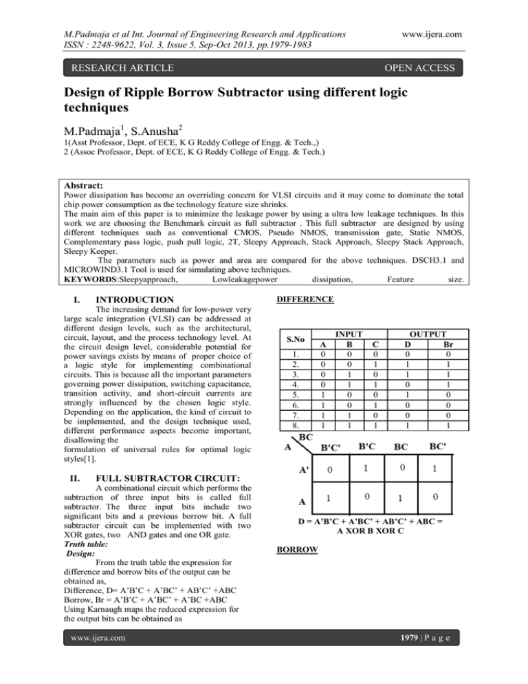
M.Padmaja et al Int. Journal of Engineering Research and Applications ISSN : 2248-9622, Vol. 3, Issue 5, Sep-Oct 2013, pp.1979-1983 www.ijera.com RESEARCH ARTICLE OPEN ACCESS Design of Ripple Borrow Subtractor using different logic techniques M.Padmaja1, S.Anusha2 1(Asst Professor, Dept. of ECE, K G Reddy College of Engg. & Tech.,) 2 (Assoc Professor, Dept. of ECE, K G Reddy College of Engg. & Tech.) Abstract: Power dissipation has become an overriding concern for VLSI circuits and it may come to dominate the total chip power consumption as the technology feature size shrinks. The main aim of this paper is to minimize the leakage power by using a ultra low leakage techniques. In this work we are choosing the Benchmark circuit as full subtractor . This full subtractor are designed by using different techniques such as conventional CMOS, Pseudo NMOS, transmission gate, Static NMOS, Complementary pass logic, push pull logic, 2T, Sleepy Approach, Stack Approach, Sleepy Stack Approach, Sleepy Keeper. The parameters such as power and area are compared for the above techniques. DSCH3.1 and MICROWIND3.1 Tool is used for simulating above techniques. KEYWORDS:Sleepyapproach, Lowleakagepower dissipation, Feature size. I. INTRODUCTION The increasing demand for low-power very large scale integration (VLSI) can be addressed at different design levels, such as the architectural, circuit, layout, and the process technology level. At the circuit design level, considerable potential for power savings exists by means of proper choice of a logic style for implementing combinational circuits. This is because all the important parameters governing power dissipation, switching capacitance, transition activity, and short-circuit currents are strongly influenced by the chosen logic style. Depending on the application, the kind of circuit to be implemented, and the design technique used, different performance aspects become important, disallowing the formulation of universal rules for optimal logic styles[1]. II. DIFFERENCE S.No 1. 2. 3. 4. 5. 6. 7. 8. A 0 0 0 0 1 1 1 1 INPUT B 0 0 1 1 0 0 1 1 C 0 1 0 1 0 1 0 1 OUTPUT D Br 0 0 1 1 1 1 0 1 1 0 0 0 0 0 1 1 FULL SUBTRACTOR CIRCUIT: A combinational circuit which performs the subtraction of three input bits is called full subtractor. The three input bits include two significant bits and a previous borrow bit. A full subtractor circuit can be implemented with two XOR gates, two AND gates and one OR gate. Truth table: Design: From the truth table the expression for difference and borrow bits of the output can be obtained as, Difference, D= A’B’C + A’BC’ + AB’C’ +ABC Borrow, Br = A’B’C + A’BC’ + A’BC +ABC Using Karnaugh maps the reduced expression for the output bits can be obtained as www.ijera.com D = A’B’C + A’BC’ + AB’C’ + ABC = A XOR B XOR C BORROW 1979 | P a g e M.Padmaja et al Int. Journal of Engineering Research and Applications ISSN : 2248-9622, Vol. 3, Issue 5, Sep-Oct 2013, pp.1979-1983 www.ijera.com on node A is a logic 1, then logic 0 is applied to node active low A allowing both transistors to conduct and pass the signal at IN to OUT. When the voltage on node active load A is a logic 0. Complementary logic 1 is applied to node A turning both transistors OFF and both transistors are open and output is high impedance. Br = A’B + A’C + BC It can also be evaluated as Br= (A xor B)’C+A’B Circuit diagram: D. Static NMOS logc: In this only two NMOS transistors are used. It reduces the count of transistors used to make different logic gates by eliminating redundant transistors. Transistors are used as switches to pass logic levels between nodes of a circuit instead of as switches connected directly to supply voltages. E. Complementary pass logic: Complementary pass logic is same as that of the static NMOS logic which is used to get both normal output and complementary output at a time. It contains total four transistors. These requires both normal outputs and complementary output to get normal and complementary output. Example: OR-NOR. Fig Full subtractor. f. Push pull logic: III. LOGIC STYLES A logic style is the way how a logic function is constructed from a set of transistors. It influences the speed, size, and power dissipation and wiring complexity of a circuit. All these characteristics may vary considerably from one logic style to another and thus make the proper choice of logic style crucial for circuit performance. A .Conventional CMOS logic: CMOS (Complementary Metal Oxide Semiconductor) consists of pull up network and pull down network. Pull up network consists only PMOS transistors and pull down network consists only NMOS transistors. Pull up network is connected between Vdd and output, and pull down network is connected between output and Vss (gnd). B. Pseudo NMOS logic: Using a PMOS transistor simply as a pull up device for an n-block is called pseudo NMOS logic. The pull up network consists of one PMOS transistor which is connected to ground and always in ON state. C. Transmission gate logic: Transmission gate belongs to CMOS logic and pass a signal level from the input to the output. This solid state switch is comprised of a PMOS transistor and NMOS transistor. The control gates are biased in a complementary manner so that both transistors are either ON or OFF when the voltage www.ijera.com Push pull logic is used to over come the disadvantage that arise in static NMOS logic and Complementary pass logic. The output drive obtained in static NMOS logic is Vdd-Vt. If we cascade the circuit it will still decreases the fan out. So, we add PMOS and NMOS transistor to the Complementary pass logic circuit. When ever PMOS is ON it pulls the logic 1(vdd) to output and NMOS transistor pushes complementary output logic 0 to output. g. 2T logic: In 2T logic only two transistors are used to design any basic gate logic. One PMOS and one NMOS transistors are used to design 2T logic. h. Sleep approach: In the sleep approach both 1. An additional sleep PMOS transistor is placed between vdd and the pull up network of a circuit. 2. An additional sleep NMOS transistor is placed between the pull down network and gnd. These sleep transistor turn off the circuit by cutting off the power rails. So, that this technique can reduce leakage power effectively. i. Stack approach: This is another technique for leakage power reduction which forces a stack effect by breaking down an existing transistor into two half size transistors. These divided transistors increases delay significantly and could limit the power dissipation. 1980 | P a g e M.Padmaja et al Int. Journal of Engineering Research and Applications ISSN : 2248-9622, Vol. 3, Issue 5, Sep-Oct 2013, pp.1979-1983 j. Sleepy stack approach: The sleepy stack approach combines the both sleep and stack approach. The sleepy stack technique divides existing transistors into two half size transistors like the stack approach. Then sleep transistor are added in parallel to one of the divided transistors. During sleep mode, sleep transistors are turned off and stacked transistors suppress leakage current while saving state. Each sleep transistor placed in parallel to the one of the stacked transistors, reduces resistance of the path. k. Sleepy keeper approach: Sleepy keeper approach utilizes leakage feedback technique. In this approach a NMOS transistor is placed in parallel to the PMOS sleep transistor and a PMOS transistor is placed in parallel to the NMOS sleep transistor. During sleep mode, sleep transistors are turned off and one of the transistor in parallel to the sleep transistors keep the connection with appropriate power rail. www.ijera.com 4-bit ripple borrow subtractor: Consider subtracting two 4-bit binary numbers, A - B or 1010 – 0111, as shown in example. We first start by considering the rightmost column (first column). A is less than B (0 < 1), thus we must borrow from the second column resulting in 10 – 1 = 1 (in base 10, two minus one equals one). In the second column, A = 0 because of the aforementioned borrow. Thus we must borrow from the third column, which intern must borrow from the fourth column. Again, once we have borrowed, the second column results in 10 – 1 = 1. In the third column, A= 01, resulting from the borrow operation generated by the second column. The third column results in 01 – 1 = 0. Lastly in the fourth column, A= 0 resulting in 0– 0 = 0. IV. APPLICATIONS By considering full subtractor as bench mark circuits the following applications are designed. They are: Ripple borrow subtractor 4-bit ripple borrow subtractor. 8-bit ripple borrow subtractor. 16-bit ripple borrow subtractor. Ripple borrow subtractor: N-bit subtractors implemented in two-level logic yield exponential growth. Thus to implement a 4bit subtractor we can break the operation down considering each column as a 1-bit subtraction operation, mimicking how we perform subtraction by hand. Here, you will build a special type of circuit called a full subtractor, as shown in Fig 6.1. The subtractor has 3 inputs: A, B, Cin, and 2 outputs: D and Bout. A and Bare the binary inputs we intend to subtract, D is the resulting binary output. In the case where B > A, we are required to borrow from previous columns, thus Bout= 1 indicating the borrow operation. In case when latter columns requires a borrow operation, Cin is set to 1. Fig 4-bit ripple borrow subtractor. Example: Sleepy keeper approach: Fig 4-bit ripple borrow subtractor using Sleepy keeper approach. Fig Full subtractor block diagram. www.ijera.com 1981 | P a g e M.Padmaja et al Int. Journal of Engineering Research and Applications ISSN : 2248-9622, Vol. 3, Issue 5, Sep-Oct 2013, pp.1979-1983 V. RESULTS Power analysis of 4-bit full subtractor using 11 techniques : Area analysis of 4-bit full subtractor using 11 techniques: Area analysis Power analysis Application Application 4-bit ripple full Subtractor Techniques 65 nm www.ijera.com 120 nm 180 nm Techniques 4-bit ripple full subtractor 65 nm 120 nm 180 nm Conventional CMOS 0.095 0.371 1.649 Conventional CMOS 198.3 3202.11 1028.008 Pseudo NMOS logic 19.526 25.073 55.793 Pseudo NMOS logic 26.08 87.67 243.5 Transmission gate logic 10.106 14.965 24.444 Transmission gate logic 53.28 238.4 2676.8 2T logic 0.151 0.201 0.806 2T logic 141.7 4130.48 11520.32 Complementary pass logic 0.275 2.379 4.835 Complementary pass 132.6 3562.67 3069.04 Static NMOS 2.259 4.426 8.141 logic Pushpull logic 9.489 17.086 29.694 Static NMOS 17.13 1675.6 10144.7 Sleep approach 0.067 0.135 0.573 Pushpull logic 240.7 3982.69 32113.18 Stack approach 0.274 0.516 3.324 Sleep approach 208.2 5394.6 15364.55 Sleepy stack approach 0.133 0.277 1.998 Stack approach 744 13911.01 38110.2 Sleepy keeper approach 0.0866 0.164 0.844 Sleepy stack approach 772.135 14570.36 14599.8 Sleepy keeper approach 330.22 1431.87 2567.5 VI. GRAPHS: 4 bit ripple borrow subtractor –area to technology graph area(um^2) 40000 35000 CONVENTIONAL CMOS 30000 PSEUDO NMOS LOGIC 25000 TRANSMISSION GATE LOGIC 20000 TWO TRANSISTOR LOGIC 15000 COMPLEMENTARY PASS LOGIC 10000 STATIC NMOS 5000 PUSH PULL LOGIC 0 SLEEP APPROACH 65nm STACK APPROACH 120nm technology www.ijera.com 180nm SLEEPY STACK APPROACH SLEEPY KEEPER APPROACH 1982 | P a g e M.Padmaja et al Int. Journal of Engineering Research and Applications ISSN : 2248-9622, Vol. 3, Issue 5, Sep-Oct 2013, pp.1979-1983 VII. CONCLUSION: Conclusion from the work carried out in this paper for implementation of adder, subtractor, adder-subtractor, we can conclude that use of static NMOS, 2T, sleepy approach provides better Improvement results in low power application than other techniques. Our circuit techniques has shown better results in Decreased power. Increased performance. Robustness. VIII. [4] [5] www.ijera.com multiplexer based decoder in flash ADC", international journal of recend trends in engineering, volume 4, may 2009, page no. 29-31. Md.AsifJahangir Chowdhary, Md.Sharhriar Rizwan and M.S.Islam, "An efficient VLSI design approach to reduce static power using variable body biasing", world academy of science, engineering and technology 64 2012, page no. 263-267. Douglas A.Pucknel kamran Eshraghian" VLSI design", 3rd edition, eastern economy edition. FUTURE SCOPE: As sleepy approach technique reduces the power delay product these can be used in high performance applications. Nowadays we are moving to ultra deep submicron technology where leakage power, area is significant. As in sleepy approach area is high, one scope is to investigate the challenging issued for designing the sleepy technique for low area occupation. REFERENCES [1] [2] [3] Harsha Vardhan Ardhan Upadayay, Abhishek Choubey, kaushalnigam "Comparision among different CMOS inverter with stack keeper approach in VLSI Design" IJERA, ISSN:2248-9622, volume 2, issue 3 may-june 2012, page no.640-646. M.Morismano, "Computer System Architecture" 3rd edition, pearson. M.S.G.L.Madhumati, Dr.M.Madhavilatha, Mr.K.Ramakoteshwara Rao "Power and Delay analysis of a 2 to 1 multiplier implemented in multiple logic styles for www.ijera.com 1983 | P a g e


