Analog Applications Journal
Industrial
Common-mode transient immunity for
isolated gate drivers
By Shailendra Baranwal
Senior Design Engineer, Isolation Team
Introduction
solar inverters, uninterruptable power supplies (UPSs), or
AC applications powered from a battery in automobiles.
The same inverter configuration allows for output-voltage
amplitude and frequency control, which is more useful for
a motor control. An induction-motor control is a common
example of using an inverter for motor control.
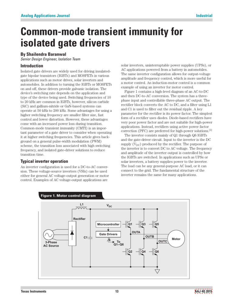
Figure 1 contains a high-level diagram of an AC-to-DC
and then DC-to-AC conversion. The system has a threephase input and controllable three-phase AC output. The
rectifier block converts the AC to DC, and a filter using L1
and C1 is used to filter out the residual ripple. A key
parameter for the rectifier is its power factor. The simplest
form of a rectifier uses diodes. Diode-based rectifiers have
very poor power factor and are not suitable for high-power
applications. Instead, rectifiers using active power factor
correction (PFC) are preferred for high-power solutions.[1]
The inverter consists mainly of Q1 through Q6 IGBTs
and the gate-driver circuit. Input to the inverter is the DC
supply (VDC) produced by the rectifier. The purpose of
the inverter is to convert DC to AC voltage. The frequency
and amplitude of the inverter output is controlled by how
the IGBTs are switched. In applications such as UPSs or
solar inverters, a battery supplies power to the inverter.
The load can be any general-purpose AC load, or it can
connect to the grid. The fundamental structure of the
inverter remains the same for many applications.
Isolated gate drivers are widely used for driving insulatedgate bipolar transistors (IGBTs) and MOSFETs in various
applications such as motor drives, solar inverters and
automobiles. In addition to turning the IGBTs or MOSFETs
on and off, these drivers provide galvanic isolation. The
device’s switching rate depends on the application and
type of the device being used. Switching frequencies of 10
to 20 kHz are common in IGBTs, however, silicon carbide
(SiC) and gallium-nitride or GaN-based systems can
operate at 50 kHz to 200 kHz. Some advantages for using a
higher switching frequency are smaller filter size, fast
control and lower distortion. However, these advantages
come with an increased power loss during transition.
Common-mode transient immunity (CMTI) is an important parameter of a gate driver to consider when operating
it at higher switching frequencies. This article gives background on a general pulse-width modulation (PWM)
scheme, the transition loss associated with high switching
frequency, and isolated gate-driver solutions to reduce
transition time.
Typical inverter operation
An inverter configuration is used for a DC-to-AC conversion. These voltage-source inverters (VSIs) can be used
either for general AC voltage-output generation or motor
control. Examples of AC voltage-output applications are
Figure 1. Motor control diagram
L1
VDC
Rectifier
Microcontroller
Gate Drivers
C1
3-Phase
AC Source
6
Q1
OUTB
OUTC
To
Q1–Q6
13
Q5
OUTA
Q2
Texas Instruments
Q3
Q4
Motor
Q6
AAJ 4Q 2015
Analog Applications Journal
Industrial
Battery-operated inverters are very common in electric
vehicles. A microcontroller is used to produce a PWM
waveform to drive the IGBTs and the outputs (OUTA,
OUTB and OUTC) switch between 0 V and VDC. An induction motor requires control of voltage and frequency to
control its torque and speed. The microcontroller monitors
the speed and current in the motor and provides the
proper PWM pattern according to user inputs. IGBTs typically require gate drivers with isolated outputs because
the output side is switching between 0 V and VDC. The
switching frequency of an IGBT-based inverter is typically
in the range of 8 to 16 kHz and higher PWM switching
frequencies are possible with SiC or GaN IGBTs.[2, 3] In this
scenario, gate drivers also need to support faster switching
speeds. The inverter can be configured as a single-phase
output with only two legs and four switches. Three-phase
systems are typically used to get more power.
Figure 2. High-level diagram of a
single-phase inverter
S1
S3
Filter
A
VAB
VDC +
–
Load
B
S2
S4
can range from 10 to 200 kHz, depending on the application and type of switch. In Figure 3a, the duty cycle at
node A is more than 50% and in Figure 3b, the duty cycle
is less than 50% at node B. This creates a positive voltage
across the load as shown in Figure 3c.
In Figure 3d, the duty cycle at node A is less than 50%
and more than 50% at node B (Figure 3e),which creates a
negative voltage across the load (Figure 3f).
The average voltage, VAB, across the load/filter can be
written as:
Pulse-width modulation
PWM or pulse-width modulation is a way to achieve amplitude control by changing the duty cycle.
Figure 2 shows a simple form of a single-phase inverter.
Input to the inverter is a DC voltage (VDC) and the voltage
across the load is VAB = VA – VB. The voltage at node A
switches between VDC and 0 V via switches S1 and S2.
Similarly, the voltage at node B switches between VDC and
0 V via switches S3 and S4. Switches S1 and S2 are
complementary, as are switches S3 and S4. The maximum
output voltage that can be achieved using this system is
VDC. An example of switching waveforms at nodes A and B
without filtering is shown in Figure 3. The switching rate
VAB = VDC × DA – VDC × DB or VAB = VDC × (DA – DB) (1)
where DA is the duty cycle at node A, and DB is duty cycle
at node B.
Figure 3. Simplified PWM operation with positive and negative output voltages
VDC
(a) VA
VDC
(d) VA
0V
0V
VDC
(b) VB
(e) VB
0V
VDC
(c)
VAB = VA – VB
0V
VDC
0V
(f)
VAB = VA – VB
0V
–VDC
Texas Instruments
14
AAJ 4Q 2015
Analog Applications Journal
Industrial
Figure 4. A single-phase PWM output waveform
INA
INB
Ramp
VA
VB
VAB
Controlling the duty cycle, DA and DB, allows control of
the output voltage, VAB. A sinusoidal single-phase PWM
waveform is obtained by comparing a reference sine wave
INA and INB with a high-frequency triangular signal as
shown in Figure 4.
The fundamental component of the output has an amplitude that is proportional to the differential reference input
(VINA – VINB), and the frequency is the same as the reference frequency. This allows the voltage and frequency to
be controlled by the reference signal. High-frequency
tones are at frequencies 2nfSW ± mfIN, where fSW is the
triangular signal frequency, fIN is the reference input
frequency, and the n and m multipliers can be 1, 2, 3, etc.
The high-frequency component is filtered by the LC filter,
or the motor inductance in the case of motor control.
The ratio between the input signal amplitude and the
triangular signal amplitude is called amplitude modulation
ratio, or mA.
mA =
VIN
VRAMP
where VIN is the amplitude of the reference input signal
and VRAMP is the amplitude of the triangular wave signal.
The fundamental output voltage is mA × VDC × sine (ωt);
where ω is the frequency of the reference input signal.
The root mean square (rms) of the fundamental signal can
be written as:
VRMS =
m A × VDC
2
(3)
Transition loss in inverters
The inverter outputs switch between ground and VDC at the
PWM frequency, however, the output current is filtered
either by the LC filter or motor inductance. Figure 5
shows waveforms for voltage and current in a PWM
switching output . Figure 5c shows a DC current with a
very small ripple component. The ripple amplitude is
dependent on the filter size. While this example shows a
DC output, the same concept can be extended for a sinewave output. However, the current is a sine wave with a
small ripple riding on it.
(2)
Figure 5. An inverter’s voltage and current waveforms with an LC filter
VDC
S1
(a) VA
S1
S3
Filter
A
VAB
VDC +
–
B
VDC
Load
S3
(b) VB
0V
S2
S2
0V
S4
S4
ILOAD
(c)
IRipple
0
Texas Instruments
15
AAJ 4Q 2015
Analog Applications Journal
Industrial
The instantaneous output power is VAB × ILOAD, where
VAB is the average DC output, which is dependent on the
duty cycles at nodes A and B. Assuming that there is no
phase difference between the voltage and current, the
output power for a sinusoidal output is:
POUT = VRMS × IRMS =
m A × VDC × IRMS
transition loss, the rise/fall time has to be lower for a
higher switching frequency. For example, a SiC-based
inverter with a 64-kHz switching frequency needs a rise/
fall time of 50 ns to keep a 1% transition loss.
Gate-drivers for Inverter
A typical drive of an IGBT-based, voltage-source inverter
is shown in Figure 6. This figure shows a single-phase
inverter, but it can be extended to a three-phase by
adding one more leg of the bridge. The voltage at outputs
OUTA or OUTB switches from VDC– to VDC+. The IGBT
gate drives are isolated because the output-side ground of
the driver is switching along with the inverter output while
the input-side ground is fixed and connected to a chassis.
The potential differences between GND1 and GND2 of
both gate drivers require the drivers to be isolated. The
gate drivers support high-voltage isolation across the two
grounds along with voltage transition rate at GND2. The
gate drivers are also selected based on their isolation
rating and their immunity to the transition on GND2, or
common-mode transient immunity (CMTI). For example,
if the DC bus is 1500 V and the transition time of OUTA is
100 ns, the immunity required by the gate driver is 15 V/ns.
The immunity requirement for the driver increases if the
rise/fall time is lower. A voltage-source inverter (VSI) with
a higher switching frequency will have a higher CMTI
requirement. A 1500-V VSI running at 64 kHz and 50-ns
rise/fall time requires at least 30-V/ns CMTI. The CMTI
requirement increases if the transition loss is to be lower.
The gate drivers are specified for CMTI in their datasheet. For example, the ISO5851 and ISO5852S both have
a minimum CMTI of 100 kV/µs. Higher CMTI for a gate
driver ensures there is no false fault or false output toggle
because of the transient noise.
The component placement or board design also matters
for a robustness to transient noise. The parasitic capacitance between one side of the driver to the other side of
the driver should be minimized. Using a diagram from the
(4)
2
The transition time from 0 V to VDC and vice versa of
the voltage at node A is finite. The switch’s ON impedance
is very low when completely on, but higher during transition time. This leads to transition-switching losses. This
loss occurs twice at every PWM cycle. Current through the
switches during transition is same as the load current
because it is filtered. Transition loss for a single event is
VDC × ILOAD × tRF / 2.
The total transition loss for a single-phase inverter is
PLOSS = 2 × 2 × fSW × ILOAD × VDC × tRF / 2
= 2 × VDC × ILOAD × tRF × fSW,
where tRF is the rise/fall time of the voltage. In case of a
sinusoidal current output, current through the switches is
an average of the load current:
2 2 × IRMS
π
and the power loss is:
(5)
I LOAD =
4 2 × VDC × I RMS × t RF × fSW
π
Ratio of the loss to output power is:
(6)
PLOSS =
PLOSS 8 × tRF × fSW
=
POUT
π × mA
(7)
Equation 6 suggests that loss is proportional to the
switching frequency. An inverter with a switching
frequency of 16 kHz and 200-ns rise/fall time will have a
1% transition loss, assuming mA = 0.8. To reduce the
Figure 6: Single-phase inverter with isolated gate drivers
GND
Texas Instruments
ISOLATION
GND1
VDC+
R1
Q1
GND2
GND1
VGEQ1
Q3
VGEQ2
OUTA
OUTB
U2
ISO5851DW
ISOLATION
Microcontroller
U1
ISO5851DW
VDC+
R2
Q2
GND2
Q4
VOUTA
VDC–
16
VDC–
AAJ 4Q 2015
Analog Applications Journal
Industrial
ISOLATION
ISO5851 datasheet,
Figure 7. Typical application where C1 and C2 can be changed to adjust CMTI
Figure 7 shows a
typical application
diagram. The Ready
10R
15
5
VCCI
VCC2
(RDY) and Fault
+ 15 V
0.1 µF
1 µF
3 to 5 V +
(FLT) pins are pulled
–
–
9,16
3
up by 10-kΩ resistors.
GND1
GND2
These resistor values
+ 15 V
1 µF
ISO5851
–
may need to be lower
10
1,8
VEE2
IN+
+
for noise immunity.
1 kΩ DDST
Transient noise can
10 kΩ
10 kΩ –
11
2
generate a false fault
IN–
DESAT
or low under-voltage
12
7
RDY
CLAMP
lockout (UVLO)
C2
RG
signal. This issue can
13
6
OUT
FLT
be solved by either
C1
reducing the resistor
14
4
NC
RST
values or increasing
the capacitance of C1
220
and C2.
pF
Digital isolators
such as the ISO7810,
ISO7821 or ISO7841
also can be used in conjunction with SiC, GaN
or IGBT drivers. Digital isolators provide reinFigure 8. Gate-driver solution using digital isolators
forced isolation and a CMTI at a minimum of
100 kV/µs. Figure 8 shows an isolated driver
VCC1
VCC2
solution using a digital isolator. The digital
V+
isolator can range from a single channel up to
+
–
U1
U2
four channels, depending on the application.
ISO7810/21/41
The digital isolator has an added benefit of
low propagation delay, low skew and low
IN
OUT
jitter, which are useful in a high-frequency
Driver
design.
Conclusion
VS
+
Voltage-source inverters (VSIs) with PWM
–
GND2
GND1
topology are a good choice for a motor
V–
control because the output amplitude and
frequency control have a lot of flexibility. A
higher switching frequency of PWM VSIs
allows for a smaller filter size. The rise/fall
3.Jang-Kwon Lim, D. Peftitsis, J. Rabkowski, M. Bakowski,
times should be lower with high switching frequencies to
H.-P. Nee, “Analysis and Experimental Verification of
keep the transition loss lower. A gate driver with good
the Influence of Fabrication Process Tolerances and
CMTI supports faster switching speeds. Gate-driver soluCircuit Parasitics on Transient Current Sharing of
tions from Texas Instruments can support a CMTI
Parallel-Connected SiC JFETs,” Power Electronics,
minimum of 100-kV/µs.
IEEE Transactions on, Volume: 29, Issue: 5, May 2014,
References
pp. 2180 – 2191
1.A. R. Prasad, P. D. Ziogas, and S. Manias, “An active
Related Web sites
power factor correction technique for three-phase diode
Product information:
rectifiers,” IEEE Trans. Power Electronics, 1991 pp.
ISO5851, ISO5852S, ISO7810, ISO7821, ISO7841
83-92
Subscribe to the AAJ:
www.ti.com/subscribe-aaj
2.Dr Scott Allen, “Silicon Carbide MOSFETs for High
Powered Modules,” CREE Inc., March 19, 2013
Texas Instruments
17
AAJ 4Q 2015
Analog Applications Journal
TI Worldwide Technical Support
Internet
TI Semiconductor Product Information Center
Home Page
support.ti.com
TI E2E™ Community Home Page
e2e.ti.com
Product Information Centers
Americas Phone
+1(512) 434-1560
Brazil
Phone
0800-891-2616
Mexico
Phone
0800-670-7544
Fax
Internet/Email
+1(972) 927-6377
support.ti.com/sc/pic/americas.htm
Europe, Middle East, and Africa
Phone
European Free Call
International
Russian Support
00800-ASK-TEXAS
(00800 275 83927)
+49 (0) 8161 80 2121
+7 (4) 95 98 10 701
Note: The European Free Call (Toll Free) number is not active in
all countries. If you have technical difficulty calling the free call
number, please use the international number above.
Fax
Internet
Direct Email
+(49) (0) 8161 80 2045
www.ti.com/asktexas
asktexas@ti.com
Japan
Fax
International
Domestic
+81-3-3344-5317
0120-81-0036
Internet/Email International
Domestic
support.ti.com/sc/pic/japan.htm
www.tij.co.jp/pic
© 2015 Texas Instruments Incorporated. All rights reserved.
Asia
Phone
Toll-Free Number
Note: Toll-free numbers may not support
mobile and IP phones.
Australia
1-800-999-084
China
800-820-8682
Hong Kong
800-96-5941
India
000-800-100-8888
Indonesia
001-803-8861-1006
Korea
080-551-2804
Malaysia
1-800-80-3973
New Zealand
0800-446-934
Philippines
1-800-765-7404
Singapore
800-886-1028
Taiwan
0800-006800
Thailand
001-800-886-0010
International +86-21-23073444
Fax
+86-21-23073686
Emailtiasia@ti.com or ti-china@ti.com
Internet
support.ti.com/sc/pic/asia.htm
Important Notice: The products and services of Texas Instruments
Incorporated and its subsidiaries described herein are sold subject to TI’s
standard terms and conditions of sale. Customers are advised to obtain the
most current and complete information about TI products and services
before placing orders. TI assumes no liability for applications assistance,
customer’s applications or product designs, software performance, or
infringement of patents. The publication of information regarding any other
company’s products or services does not constitute TI’s approval, warranty
or endorsement thereof.
A021014
E2E is a trademark of Texas Instruments. All other trademarks are the ­property of
their respective owners.
SLYT648
IMPORTANT NOTICE
Texas Instruments Incorporated and its subsidiaries (TI) reserve the right to make corrections, enhancements, improvements and other
changes to its semiconductor products and services per JESD46, latest issue, and to discontinue any product or service per JESD48, latest
issue. Buyers should obtain the latest relevant information before placing orders and should verify that such information is current and
complete. All semiconductor products (also referred to herein as “components”) are sold subject to TI’s terms and conditions of sale
supplied at the time of order acknowledgment.
TI warrants performance of its components to the specifications applicable at the time of sale, in accordance with the warranty in TI’s terms
and conditions of sale of semiconductor products. Testing and other quality control techniques are used to the extent TI deems necessary
to support this warranty. Except where mandated by applicable law, testing of all parameters of each component is not necessarily
performed.
TI assumes no liability for applications assistance or the design of Buyers’ products. Buyers are responsible for their products and
applications using TI components. To minimize the risks associated with Buyers’ products and applications, Buyers should provide
adequate design and operating safeguards.
TI does not warrant or represent that any license, either express or implied, is granted under any patent right, copyright, mask work right, or
other intellectual property right relating to any combination, machine, or process in which TI components or services are used. Information
published by TI regarding third-party products or services does not constitute a license to use such products or services or a warranty or
endorsement thereof. Use of such information may require a license from a third party under the patents or other intellectual property of the
third party, or a license from TI under the patents or other intellectual property of TI.
Reproduction of significant portions of TI information in TI data books or data sheets is permissible only if reproduction is without alteration
and is accompanied by all associated warranties, conditions, limitations, and notices. TI is not responsible or liable for such altered
documentation. Information of third parties may be subject to additional restrictions.
Resale of TI components or services with statements different from or beyond the parameters stated by TI for that component or service
voids all express and any implied warranties for the associated TI component or service and is an unfair and deceptive business practice.
TI is not responsible or liable for any such statements.
Buyer acknowledges and agrees that it is solely responsible for compliance with all legal, regulatory and safety-related requirements
concerning its products, and any use of TI components in its applications, notwithstanding any applications-related information or support
that may be provided by TI. Buyer represents and agrees that it has all the necessary expertise to create and implement safeguards which
anticipate dangerous consequences of failures, monitor failures and their consequences, lessen the likelihood of failures that might cause
harm and take appropriate remedial actions. Buyer will fully indemnify TI and its representatives against any damages arising out of the use
of any TI components in safety-critical applications.
In some cases, TI components may be promoted specifically to facilitate safety-related applications. With such components, TI’s goal is to
help enable customers to design and create their own end-product solutions that meet applicable functional safety standards and
requirements. Nonetheless, such components are subject to these terms.
No TI components are authorized for use in FDA Class III (or similar life-critical medical equipment) unless authorized officers of the parties
have executed a special agreement specifically governing such use.
Only those TI components which TI has specifically designated as military grade or “enhanced plastic” are designed and intended for use in
military/aerospace applications or environments. Buyer acknowledges and agrees that any military or aerospace use of TI components
which have not been so designated is solely at the Buyer's risk, and that Buyer is solely responsible for compliance with all legal and
regulatory requirements in connection with such use.
TI has specifically designated certain components as meeting ISO/TS16949 requirements, mainly for automotive use. In any case of use of
non-designated products, TI will not be responsible for any failure to meet ISO/TS16949.
Products
Applications
Audio
www.ti.com/audio
Automotive and Transportation
www.ti.com/automotive
Amplifiers
amplifier.ti.com
Communications and Telecom
www.ti.com/communications
Data Converters
dataconverter.ti.com
Computers and Peripherals
www.ti.com/computers
DLP® Products
www.dlp.com
Consumer Electronics
www.ti.com/consumer-apps
DSP
dsp.ti.com
Energy and Lighting
www.ti.com/energy
Clocks and Timers
www.ti.com/clocks
Industrial
www.ti.com/industrial
Interface
interface.ti.com
Medical
www.ti.com/medical
Logic
logic.ti.com
Security
www.ti.com/security
Power Mgmt
power.ti.com
Space, Avionics and Defense
www.ti.com/space-avionics-defense
Microcontrollers
microcontroller.ti.com
Video and Imaging
www.ti.com/video
RFID
www.ti-rfid.com
OMAP Applications Processors
www.ti.com/omap
TI E2E Community
e2e.ti.com
Wireless Connectivity
www.ti.com/wirelessconnectivity
Mailing Address: Texas Instruments, Post Office Box 655303, Dallas, Texas 75265
Copyright © 2015, Texas Instruments Incorporated
