US5881
Unipolar Hall Switch – Lo
Low Sensitivity
Features and Benefits
Application Exam
mples
Wide operating voltage range frrom 3.5V to
24V
Low sensitivity
CMOS technology
Chopper-stabilized amplifier stage
tage
Low current consumption
Open drain output
Thin SOT23 3L and flat TO-92 3L
both RoHS Compliant
packages
Automotive, Consu
umer and Industrial
Solid-state switch
Interrupter
Current detector
Proximity detection
on
Ordering Code
Product Code
US5881
US5881
US5881
US5881
Temperature Code
E
L
E
L
Legend:
Temperature Code:
Package Code
UA
UA
SE
SE
Option Code
AAA-000
AAA-000
AAA-000
AAA-000
Package Code:
Packing Form:
L for Temperature Range -40°C to 150°C
E for Temperature Range -40°C to 85°C
UA for TO-92(Flat),
92(Flat), SE for TSOT3
RE for Reel, BU for Bulk
Ordering example:
US5881EUA-AAA
AAA-000-BU
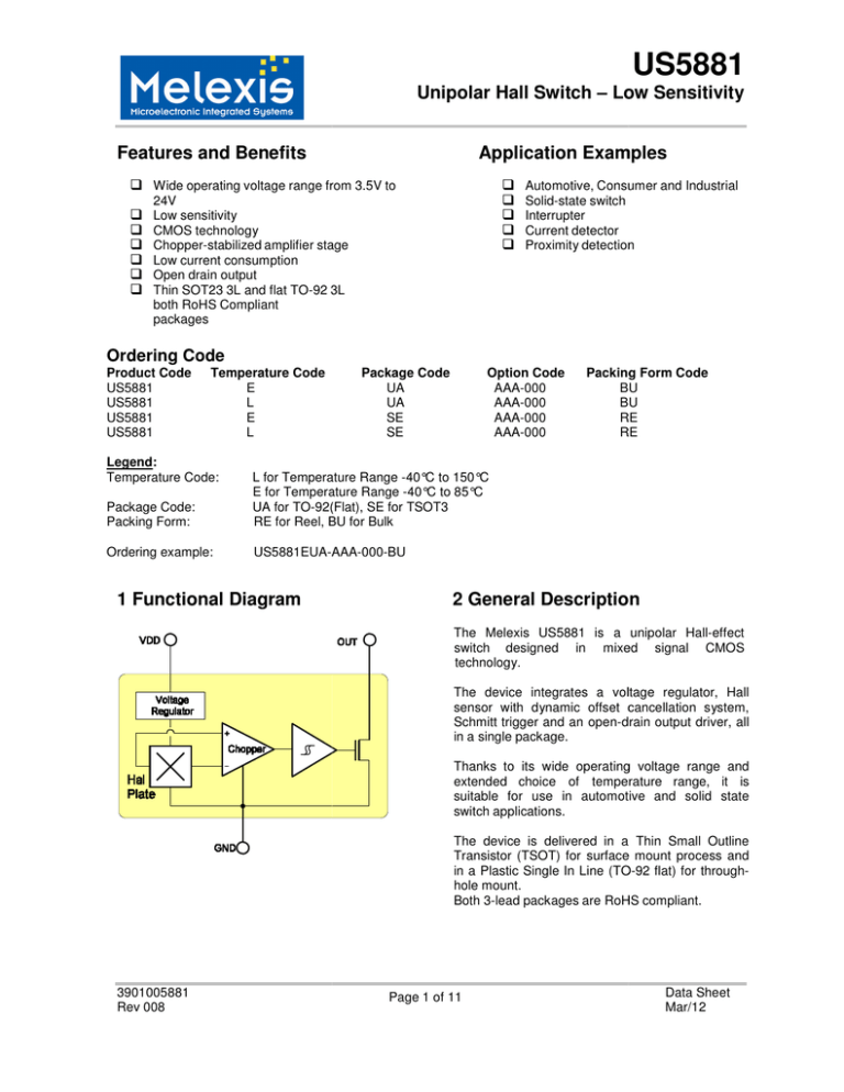
1 Functional Diagram
Packing Form Code
BU
BU
RE
RE
2 General Descriptio
ion
The Melexis US5881 is a unipolar Hall-effect
switch designed in mixed
ed signal CMOS
technology.
The device integrates a volltage regulator, Hall
sensor with dynamic offset ccancellation system,
Schmitt trigger and an open-d
drain output driver, all
in a single package.
Thanks to its wide operating
ng voltage range and
extended choice of temperrature range, it is
suitable for use in automot
otive and solid state
switch applications.
The device is delivered in a Thin Small Outline
Transistor (TSOT) for surface
e mount process and
in a Plastic Single In Line (TO
O-92 flat) for throughhole mount.
Both 3-lead packages are RoHS compliant.
3901005881
Rev 008
Page 1 of 11
Data Sheet
Mar/12
US5881
Unipolar Hall Switch – Low Sensitivity
Table of Contents
1 Functional Diagram ........................................................................................................ 1
2 General Description ........................................................................................................ 1
3 Glossary of Terms .......................................................................................................... 3
4 Absolute Maximum Ratings ........................................................................................... 3
5 Pin Definitions and Descriptions ................................................................................... 3
6 General Electrical Specifications .................................................................................. 4
7 Magnetic Specifications ................................................................................................. 4
8 Output Behaviour versus Magnetic Pole ...................................................................... 4
9 Detailed General Description ......................................................................................... 5
10 Unique Features ............................................................................................................ 5
11 Performance Graphs .................................................................................................... 6
11.1 Typical Magnetic Switch Points vs VDD ....................................................................................................6
11.2 Magnetic Switch Points vs Temperature .................................................................................................6
11.3 Typical Supply Current vs VDD .................................................................................................................6
11.4 Typical Saturation Voltage vc Temperature (VDD=12V; Iout=20mA) .....................................................6
12 Application Information................................................................................................ 7
12.1 Typical Three-Wire Application Circuit ....................................................................................................7
12.2 Two-Wire Circuit ......................................................................................................................................7
12.3 Automotive and Harsh, Noisy Environments Three-Wire Circuit ............................................................7
13 Application Comments ................................................................................................. 7
14 Standard information regarding manufacturability of Melexis products with
different soldering processes........................................................................................... 8
15 ESD Precautions ........................................................................................................... 8
16 Package Information..................................................................................................... 9
16.1 SE Package (TSOT-3L)...........................................................................................................................9
16.2 UA Package (TO-92 flat) .......................................................................................................................10
17 Disclaimer.................................................................................................................... 11
3901005881
Rev 008
Page 2 of 11
Data Sheet
Mar/12
US5881
Unipolar Hall Switch – Low Sensitivity
3 Glossary of Terms
MilliTesla (mT), Gauss
RoHS
TSOT
ESD
BLDC
Units of magnetic flux density:
1mT = 10 Gauss
Restriction of Hazardous Substances
Thin Small Outline Transistor (TSOT package) – also referred with the Melexis
package code “SE”
Electro-Static Discharge
Brush-Less Direct-Current
4 Absolute Maximum Ratings
Parameter
Symbol
Supply Voltage
VDD
Supply Current
IDD
Output Voltage
VOUT
Output Current
IOUT
Storage Temperature Range
TS
Maximum Junction Temperature
TJ
Table 1: Absolute maximum ratings
Value
28
50
28
50
-50 to 150
165
Units
V
mA
V
mA
°C
°C
Exceeding the absolute maximum ratings may cause permanent damage. Exposure to absolute-maximumrated conditions for extended periods may affect device reliability.
Operating Temperature Range
Temperature Suffix “E”
Temperature Suffix “L”
Symbol
TA
TA
Value
-40 to 85
-40 to 150
Units
°C
°C
5 Pin Definitions and Descriptions
SE Pin № UA Pin № Name
1
1
VDD
2
3
OUT
3
2
GND
Table 2: Pin definitions and descriptions
SE package
3901005881
Rev 008
Type
Supply
Output
Ground
Function
Supply Voltage pin
Open Drain Output pin
Ground pin
UA package
Page 3 of 11
Data Sheet
Mar/12
US5881
Unipolar Hall Switch – Low Sensitivity
6 General Electrical Specifications
DC Operating Parameters T A = 25oC, VDD
Parameter
Symbol
Supply Voltage
VDD
Supply Current
IDD
Output Saturation Voltage
VDSon
Output Leakage Current
IOFF
Output Rise Time
tr
Output Fall Time
tf
Maximum Switching Frequency
FSW
SE Package Thermal Resistance
RTH
UA Package Thermal Resistance
RTH
Table 3: Electrical specifications
= 12V (unless otherwise specified)
Test Conditions
Min
Operating
3.5
B < BRP
1.5
IOUT = 20mA, B > BOP
B < BRP, VOUT = 24V
RL = 1kΩ, CL = 20pF
RL = 1kΩ, CL = 20pF
Single layer (1S) Jedec board
Typ
2.5
0.4
0.01
0.25
0.25
10
301
200
Max
24
5
0.5
10
Units
V
mA
V
µA
µs
µs
KHz
°C/W
°C/W
7 Magnetic Specifications
DC Operating Parameters T A = 25oC, VDD = 12V (unless otherwise specified)
Parameter
Symbol
Test Conditions
Min
Typ
Operating Point
BOP
15
25
Release Point
BRP
9.5
20
Hysteresis
BHYST
2
4.3
Table 4: Magnetic specifications
Max
30
5.5
Units
mT
mT
mT
8 Output Behaviour versus Magnetic Pole
DC Operating Parameters TA = -40 oC to 150 oC, VDD = 3.5V to 24V (unless otherwise specified)
Parameter
Test Conditions (SE) OUT (SE) OUT (UA)
South pole
B > BOP
High
Low
Null or weak magnetic field
B -7 0 or B < BRP
High
High
North pole
B > BOP
Low
High
Table 5: Output behaviour versus magnetic pole
North pole
South pole
OUT = low (VDSon)
SE package
3901005881
Rev 008
OUT = low (VDSon)
UA package
Page 4 of 11
Data Sheet
Mar/12
US5881
Unipolar Hall Switch – Lo
Low Sensitivity
9 Detailed General Descri
ription
Based on mixed signal CMOS technology, Melexis US5881 is a Hall-effect device with low
w magnetic
sensitivity. Its sensitivity enables high accuracy in position sensing by the use of small air g
gap.
The chopper-stabilized amplifier uses switched capacitor technique to suppress the offset generally observed
with Hall sensors and amplifiers. The CMOS
CM
technology makes this advanced technique possible
po
and
contributes to smaller chip size and lo
ower current consumption than bipolar technology. The
he small chip size is
also an important factor to minimize th
he effect of physical stress.
This combination results in more stablle magnetic characteristics and enables faster and more
m
precise design.
The wide operating voltage from 3.5V to 24V, “L” and “E” operating temperature range and
d low current
consumption make this device especia
ally suitable for automotive solid state switch applica
ations.
The output signal is open-drain type. Such
S
output allows simple connectivity with TTL or CMOS
CM
logic by using
a pull-up resistor tied between a pull-u
up voltage and the device output.
10 Unique Features
The US5881 exhibits unipolar magnet
agnetic switching characteristics. Therefore, it operates on
nly with one
magnetic pole.
The UA package is south pole active:
Applying a south magnetic pole greater than BOP facing the
branded side of the package switches the outp
put low.
The SE package is north pole active:
Applying a north magnetic pole greater than BOP facing the
branded side of the package switches the outp
put low.
Unipolar switch characteristic
Removing the magnetic field (B→0) switches the output high.
The use of the opposite magnetic pole facing the branded side
does not affect the output state.
A magnetic hysteresis BHYST keeps BOP and BRP separated by a minimal value. This hysterresis prevents
output oscillation near the switching point.
po
3901005881
Rev 008
Page 5 of 11
Data Sheet
Mar/12
US5881
Unipolar Hall Switch – Lo
Low Sensitivity
11 Performance Graphs
11.2 Magnetic Switch Poiints vs
Temperature
11.3 Typical Supply Current vs
v VDD
11.4 Typical Saturation Voltage
V
vc
Temperature (VDD=1
=12V; Iout=20mA)
Supply Current (mA)
11.1 Typical Magnetic Switch Points vs
VDD
3901005881
Rev 008
Page 6 of 11
Data Sheet
Mar/12
US5881
Unipolar Hall Switch – Lo
Low Sensitivity
12 Application Informatio
on
12.1 Typical Three-Wire Applica
lication Circuit
12.2 Two-Wire
re Circuit
12.3 Automotive and Harsh, Noisy
No
Environments
Three-Wire Circuit
Note:
With this circuit, p
precise ON and OFF
currents can be de
detected using only
two connecting wiires.
The resistors RL and
a Rb can be used
to bias the input ccurrent. Refer to the
part specifications
ons for limiting values.
BRP :
BOP :
IOFF = IR + IDD = VDD/Rb + IDD
ION = IOFF + IOUT = IOFF + VDD/RL
13 Application Comments
ts
For proper operation, a 100nF bypass
s capacitor should be placed as close as possible to tthe device between
the VDD and ground pin.
For reverse voltage protection, it is rec
commended to connect a resistor or a diode in series
es with the VDD pin.
When using a resistor, three points are
e important:
- the resistor has to limit the re
everse current to 50mA maximum (VCC / R1 ≤ 50mA))
- the resulting device supply voltage
v
VDD has to be higher than VDD min (VDD = VCCC – R1.IDD)
- the resistor has to withstand
nd the power dissipated in reverse voltage condition (P
PD = VCC 2 / R1)
When using a diode, a reverse current
ent cannot flow and the voltage drop is almost constant
tant (≈0.7V).
Therefore, a 100Ω/0.25W resistor for 5V application and a diode for higher supply voltage
e are recommended.
Both solutions provide the required revverse voltage protection.
When a weak power supply is used or when the device is intended to be used in noisy envi
vironment, it is
recommended that figure 13.3 from the Application Information section is used.
The low-pass filter formed by R1 and C1
C and the zener diode Z1 bypass the disturbances or voltage spikes
occurring on the device supply voltage
age VDD. The diode D1 provides additional reverse volta
tage protection.
3901005881
Rev 008
Page 7 of 11
Data Sheet
Mar/12
US5881
Unipolar Hall Switch – Low Sensitivity
14 Standard information regarding manufacturability of Melexis
products with different soldering processes
Our products are classified and qualified regarding soldering technology, solderability and moisture
sensitivity level according to following test methods:
Reflow Soldering SMD’s (Surface Mount Devices)
•
•
IPC/JEDEC J-STD-020
Moisture/Reflow Sensitivity Classification for Nonhermetic Solid State Surface Mount Devices
(classification reflow profiles according to table 5-2)
EIA/JEDEC JESD22-A113
Preconditioning of Nonhermetic Surface Mount Devices Prior to Reliability Testing
(reflow profiles according to table 2)
Wave Soldering SMD’s (Surface Mount Devices) and THD’s (Through Hole Devices)
•
•
EN60749-20
Resistance of plastic- encapsulated SMD’s to combined effect of moisture and soldering heat
EIA/JEDEC JESD22-B106 and EN60749-15
Resistance to soldering temperature for through-hole mounted devices
Iron Soldering THD’s (Through Hole Devices)
•
EN60749-15
Resistance to soldering temperature for through-hole mounted devices
Solderability SMD’s (Surface Mount Devices) and THD’s (Through Hole Devices)
•
EIA/JEDEC JESD22-B102 and EN60749-21
Solderability
For all soldering technologies deviating from above mentioned standard conditions (regarding peak
temperature, temperature gradient, temperature profile etc) additional classification and qualification
tests have to be agreed upon with Melexis.
The application of Wave Soldering for SMD’s is allowed only after consulting Melexis regarding
assurance of adhesive strength between device and board.
Melexis is contributing to global environmental conservation by promoting lead free solutions. For
more information on qualifications of RoHS compliant products (RoHS = European directive on the
Restriction Of the use of certain Hazardous Substances) please visit the quality page on our website:
http://www.melexis.com/quality.aspx
15 ESD Precautions
Electronic semiconductor products are sensitive to Electro Static Discharge (ESD).
Always observe Electro Static Discharge control procedures whenever handling semiconductor products.
3901005881
Rev 008
Page 8 of 11
Data Sheet
Mar/12
US5881
Unipolar Hall Switch – Lo
Low Sensitivity
16 Package Information
0.127 +0.023
- 0.007
0.891 +/-0.05
0.20
0.15
0.20
1.90 BSC
0.30
0.45
0.95 BSC
see note 3
2.90 BSC
16.1 SE Package (TSOT-3L)
3901005881
Rev 008
Page 9 of 11
Data Sheet
Mar/12
US5881
Unipolar Hall Switch – Lo
Low Sensitivity
14.5+/-0.5
2.5 min
see note 4
1.65+/-0.10
3.00+/-0.20
16.2 UA Package (TO-92 flat)
3901005881
Rev 008
Page 10 of 11
Data Sheet
Mar/12
US5881
Unipolar Hall Switch – Low Sensitivity
17 Disclaimer
Devices sold by Melexis are covered by the warranty and patent indemnification provisions appearing
in its Term of Sale. Melexis makes no warranty, express, statutory, implied, or by description regarding
the information set forth herein or regarding the freedom of the described devices from patent
infringement. Melexis reserves the right to change specifications and prices at any time and without
notice. Therefore, prior to designing this product into a system, it is necessary to check with Melexis for
current information. This product is intended for use in normal commercial applications. Applications
requiring extended temperature range, unusual environmental requirements, or high reliability
applications, such as military, medical life-support or life-sustaining equipment are specifically not
recommended without additional processing by Melexis for each application.
The information furnished by Melexis is believed to be correct and accurate. However, Melexis shall
not be liable to recipient or any third party for any damages, including but not limited to personal injury,
property damage, loss of profits, loss of use, interrupt of business or indirect, special incidental or
consequential damages, of any kind, in connection with or arising out of the furnishing, performance or
use of the technical data herein. No obligation or liability to recipient or any third party shall arise or
flow out of Melexis’ rendering of technical or other services.
© 2012 Melexis NV. All rights reserved.
For the latest version of this document, go to our website at
www.melexis.com
Or for additional information contact Melexis Direct:
Europe, Africa, Asia:
Phone: +32 1367 0495
E-mail: sales_europe@melexis.com
America:
Phone: +1 248 306 5400
E-mail: sales_usa@melexis.com
ISO/TS 16949 and ISO14001 Certified
3901005881
Rev 008
Page 11 of 11
Data Sheet
Mar/12
