US5683
Unipolar Hall Switch – High Sensitivity
Inverted Output
Features and Benefits
Application Examples
Wide operating voltage range from 3.5V to 24V
High sensitivity
CMOS technology
Chopper-stabilized amplifier stage
Low current consumption
Open drain output
Inverted Output
Thin SOT23 3L RoHS Compliant package
Automotive, Consumer and Industrial
Solid-state switch
Interrupter
Current detector
Proximity detection
Ordering Information
Product Code
Temperature
Code
E, K
US5683
Legend:
Temperature Code:
Package Code:
Option Code:
Packing Form:
Ordering example:
OUT
DIG
POR
Temperature
compensation
DAMP
Hall
Plate
GND
3901005683
Rev 005
SE
AAA-000
Packing Form
Code
RE
2 General Description
VDD
ESD protection
Option Code
E(-40°C to 85°C) K(-40°C to 125°C)
SE =TSOT-23L
AAA-000
RE=Reel
US5683ESE-AAA-000-RE
1 Functional Diagram
Voltage
Regulator
Package Code
Oscillator and
Bias
ESD protection
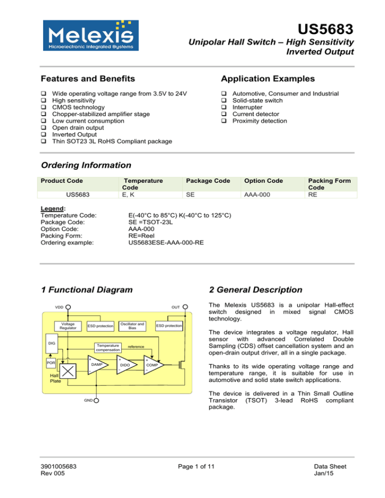
The device integrates a voltage regulator, Hall
sensor with advanced Correlated Double
Sampling (CDS) offset cancellation system and an
open-drain output driver, all in a single package.
reference
DIDO
The Melexis US5683 is a unipolar Hall-effect
switch designed in mixed signal CMOS
technology.
COMP
Thanks to its wide operating voltage range and
temperature range, it is suitable for use in
automotive and solid state switch applications.
The device is delivered in a Thin Small Outline
Transistor (TSOT) 3-lead RoHS compliant
package.
Page 1 of 11
Data Sheet
Jan/15
US5683
Unipolar Hall Switch – High Sensitivity
Inverted Output
Table of Contents
1 Functional Diagram ........................................................................................................ 1
2 General Description ........................................................................................................ 1
3 Glossary of Terms .......................................................................................................... 3
4 Absolute Maximum Ratings ........................................................................................... 3
5 Pin Definitions and Descriptions ................................................................................... 3
6 General Electrical Specifications .................................................................................. 4
7 Magnetic Specifications ................................................................................................. 4
8 Output Behaviour versus Magnetic Pole ...................................................................... 5
9 Detailed General Description ......................................................................................... 5
10 Unique Features ............................................................................................................ 5
11 Performance Graphs .................................................................................................... 6
12 Test Conditions ............................................................................................................. 7
13 Application Information ................................................................................................ 8
13.1 Typical Three-Wire Application Circuit ...................................................................... 8
13.2 Two-Wire Circuit ....................................................................................................... 8
13.3 Automotive and Harsh, Noisy Environments Three-Wire Circuit ............................... 8
14 Application Comments ................................................................................................. 8
15 Standard information regarding manufacturability of Melexis products with
different soldering processes ........................................................................................... 9
16 ESD Precautions ........................................................................................................... 9
17 SE Package Information (TSOT-3L) ........................................................................... 10
18 Disclaimer .................................................................................................................... 11
3901005683
Rev 005
Page 2 of 11
Data Sheet
Jan/15
US5683
Unipolar Hall Switch – High Sensitivity
Inverted Output
3 Glossary of Terms
MilliTesla (mT), Gauss
RoHS
TSOT
ESD
Units of magnetic flux density:
1mT = 10 Gauss
Restriction of Hazardous Substances
Thin Small Outline Transistor (TSOT package) – also referred with the Melexis
package code “SE”
Electro-Static Discharge
4 Absolute Maximum Ratings
Parameter
Symbol
Supply Voltage
VDD
Supply Current
IDD
Output Voltage
VOUT
Output Current
IOUT
Operating Temperature Range
TA
Storage Temperature Range
TS
Maximum Junction Temperature
TJ
ESD Sensitivity – HBM (1)
Table 1: Absolute maximum ratings
Value
28
50
28
50
-40 to 125
-50 to 150
165
2000
Units
V
mA
V
mA
C
C
C
V
Exceeding the absolute maximum ratings may cause permanent damage. Exposure to absolute-maximumrated conditions for extended periods may affect device reliability.
1
Human Body Model according AEC-Q100-002 standard.
5 Pin Definitions and Descriptions
Pin №
Name
Type
1
VDD
Supply
2
OUT
Output
3
GND
Ground
Table 2: Pin definitions and descriptions
3901005683
Rev 005
Function
Supply Voltage pin
Open Drain Output pin
Ground pin
Page 3 of 11
Data Sheet
Jan/15
US5683
Unipolar Hall Switch – High Sensitivity
Inverted Output
6 General Electrical Specifications
o
DC Operating Parameters TA = 25 C, VDD = 12V (unless otherwise specified)
Parameter
Symbol
Supply Voltage
VDD
Supply Current
IDD
Output Saturation Voltage
VDSon
Output Leakage Current
IOFF
Output Rise Time
tr
Output Fall Time
tf
Maximum Switching Frequency
FSW
Power-On Time (2)
tON
Package Thermal Resistance
RTH
Table 3: Electrical specifications
Test Conditions
Operating
B < BRP
IOUT = 20mA, B < BRP
B > BOP, VOUT = 24V
RL = 1k, CL = 20pF
RL = 1k, CL = 20pF
Min
3.5
0.5
Typ
2.5
0.3
0.01
0.25
0.25
5
Max
24
5
0.5
10
100
Single layer (1S) Jedec board
301
Units
V
mA
V
A
s
s
KHz
s
°C/W
2
The Power-On Time represents the time from reaching the power-on reset level to the first refresh of the
output (first valid output state).Value according simulation only, not subject to production test.
7 Magnetic Specifications
o
DC Operating Parameters TA = 25 C, VDD = 12V (unless otherwise specified)
Parameter
Symbol
Operating Point
BOP
Release Point
BRP
Hysteresis
BHYST
Table 4: Magnetic specifications
o
Test Conditions
Min
3.8
2
1.5
Typ
5.5
3.5
2
Max
7.2
5
2.7
Units
mT
mT
mT
Max
7.7
5.4
2.8
Units
mT
mT
mT
o
DC Operating Parameters TA = -40 C to 125 C, VDD = 12V (unless otherwise specified)
Parameter
Symbol
Operating Point
BOP
Release Point
BRP
Hysteresis
BHYST
Table 5: Magnetic specifications
3901005683
Rev 005
Test Conditions
Page 4 of 11
Min
3.4
1.8
1
Typ
Data Sheet
Jan/15
US5683
Unipolar Hall Switch – High Sensitivity
Inverted Output
8 Output Behaviour versus Magnetic Pole
o
o
DC Operating Parameters TA = -40 C to 125 C, VDD = 12V
Parameter
Test Conditions
North pole
B > BOP
Null or weak magnetic field
B 0 or B < BRP
South pole
B > BOP
Table 6: Output behaviour versus magnetic pole
OUT
High
Low
Low
OUT = High (≈VPU)
9 Detailed General Description
Based on mixed signal CMOS technology, Melexis US5683 is a Hall-effect device with high magnetic
sensitivity and inverted output. Its sensitivity enables high accuracy in position sensing by the use of small air
gap.
The Correlated Double Sampling (CDS) technique suppresses the offset generally observed with Hall
sensors and amplifiers. The CMOS technology makes this advanced technique possible and contributes to
smaller chip size and lower current consumption than bipolar technology. The small chip size is also an
important factor to minimize the effect of physical stress.
This combination results in more accurate and stable magnetic characteristics, and enables faster and more
precise design.
The wide operating voltage from 3.5V to 24V and low current consumption make this device especially
suitable for solid state switch applications.
The output signal is open-drain type. Such output allows simple connectivity with TTL or CMOS logic by using
a pull-up resistor tied between a pull-up voltage and the device output.
10 Unique Features
The US5683 exhibits unipolar magnetic switching characteristics. Therefore, it operates only with one
magnetic pole.
Output level
OUT switches to High
OUT switches to Low
OUT = High
The US5683 device is inverted output, north pole active:
Applying a north magnetic pole greater than BOP facing the
branded side of the package switches the output high.
Removing the magnetic field (B0) switches the output low.
The use of the opposite magnetic pole facing the branded side
does not affect the output state.
OUT = Low
0mT
BOP
Flux density
BRP
Unipolar switch characteristic
A magnetic hysteresis BHYST keeps BOP and BRP separated by a minimal value. This hysteresis prevents
output oscillation near the switching point.
3901005683
Rev 005
Page 5 of 11
Data Sheet
Jan/15
US5683
Unipolar Hall Switch – High Sensitivity
Inverted Output
11 Performance Graphs
11.1 Magnetic parameters vs. TA
11.2 Magnetic parameters vs. VDD
11.3 VDSon vs. TA
11.4 VDSon vs. VDD
11.5 IDD vs. TA
11.6 IDD vs. VDD
3901005683
Rev 005
Page 6 of 11
Data Sheet
Jan/15
US5683
Unipolar Hall Switch – High Sensitivity
Inverted Output
12 Test Conditions
Note : DUT = Device Under Test
12.1 Supply Current
IDD
A
VDD
12.2 Output Saturation Voltage
OUT
VDD
DUT
OUT
DUT
VDD
GND
Note 1 - The supply current IDD represents the static supply current.
OUT is left open during measurement.
Note 2 - The device is put under magnetic field with B<BRP.
12.3 Output Leakage Current
VDD
VDD
3.5 / 24V
DUT
Note 2 - The device is put under magnetic field with B<BRP.
12.4 Magnetic Thresholds
10Kohms
A
VDD
24V
VDD
VDSon
Note 1 - The output saturation voltage VDSon is measured
at VDD = 3.5V and VDD = 24V.
IOFF
OUT
V
20mA
GND
DUT
OUT
V
VDD
GND
GND
Note 1 - The device is put under magnetic field with B>BOP
Note 1 - BOP is determined by putting the device under magnetic field swept from
BRPmin up to BOPmax until the output is switched on.
Note 2 - BRPis determined by putting the device under magnetic field swept from
BOPmax down to BRPmin until the output is switched off.
3901005683
Rev 005
Page 7 of 11
Data Sheet
Jan/15
US5683
Unipolar Hall Switch – High Sensitivity
Inverted Output
13 Application Information
13.1 Typical Three-Wire Application Circuit
13.2 Two-Wire Circuit
VDD
VCC
C1
100nF
RPU
10k
VDD
IIN
IR
VOUT
OUT
VSS
IOUT
IDD
C2
4.7nF
Rb
RL*
VDD
OUT
VSS
13.3 Automotive and Harsh, Noisy Environments
Three-Wire Circuit
D1
VCC
Note:
With this circuit, precise ON and OFF
currents can be detected using only
two connecting wires.
R1
RPU
100 Ohms
10k
VDD
Z1
C1
VOUT
OUT
100nF
VSS
C2
The resistors RL and Rb can be used
to bias the input current. Refer to the
part specifications for limiting values.
4.7nF
BRP :
BOP :
IOFF = IR + IDD = VDD/Rb + IDD
ION = IOFF + IOUT = IOFF + VDD/RL
14 Application Comments
For proper operation, a 100nF bypass capacitor should be placed as close as possible to the device between
the VDD and ground pin.
For reverse voltage protection, it is recommended to connect a resistor or a diode in series with the VDD pin.
When using a resistor, three points are important:
- the resistor has to limit the reverse current to 50mA maximum (VCC / R1 50mA)
- the resulting device supply voltage VDD has to be higher than VDD min (VDD = VCC – R1.IDD)
2
- the resistor has to withstand the power dissipated in reverse voltage condition (P D = VCC / R1)
When using a diode, a reverse current cannot flow and the voltage drop is almost constant (0.7V).
Therefore, a 100/0.25W resistor for 5V application and a diode for higher supply voltage are recommended.
Both solutions provide the required reverse voltage protection.
When a weak power supply is used or when the device is intended to be used in noisy environment, it is
recommended that figure 13.3 from the Application Information section is used.
The low-pass filter formed by R1 and C1 and the zener diode Z1 bypass the disturbances or voltage spikes
occurring on the device supply voltage VDD. The diode D1 provides additional reverse voltage protection.
3901005683
Rev 005
Page 8 of 11
Data Sheet
Jan/15
US5683
Unipolar Hall Switch – High Sensitivity
Inverted Output
15 Standard information regarding manufacturability of Melexis
products with different soldering processes
Our products are classified and qualified regarding soldering technology, solderability and moisture sensitivity
level according to following test methods:
Reflow Soldering SMD’s (Surface Mount Devices)
IPC/JEDEC J-STD-020
Moisture/Reflow Sensitivity Classification for Nonhermetic Solid State Surface Mount Devices
(classification reflow profiles according to table 5-2)
EIA/JEDEC JESD22-A113
Preconditioning of Nonhermetic Surface Mount Devices Prior to Reliability Testing
(reflow profiles according to table 2)
Wave Soldering SMD’s (Surface Mount Devices) and THD’s (Through Hole Devices)
EN60749-20
Resistance of plastic- encapsulated SMD’s to combined effect of moisture and soldering heat
EIA/JEDEC JESD22-B106 and EN60749-15
Resistance to soldering temperature for through-hole mounted devices
Iron Soldering THD’s (Through Hole Devices)
EN60749-15
Resistance to soldering temperature for through-hole mounted devices
Solderability SMD’s (Surface Mount Devices) and THD’s (Through Hole Devices)
EIA/JEDEC JESD22-B102 and EN60749-21
Solderability
For all soldering technologies deviating from above mentioned standard conditions (regarding peak
temperature, temperature gradient, temperature profile etc) additional classification and qualification tests
have to be agreed upon with Melexis.
The application of Wave Soldering for SMD’s is allowed only after consulting Melexis regarding assurance of
adhesive strength between device and board.
Melexis is contributing to global environmental conservation by promoting lead free solutions. For more
information on qualifications of RoHS compliant products (RoHS = European directive on the Restriction Of
the use of certain Hazardous Substances) please visit the quality page on our website:
http://www.melexis.com/quality.aspx
16 ESD Precautions
Electronic semiconductor products are sensitive to Electro Static Discharge (ESD).
Always observe Electro Static Discharge control procedures whenever handling semiconductor products.
3901005683
Rev 005
Page 9 of 11
Data Sheet
Jan/15
US5683
Unipolar Hall Switch – High Sensitivity
Inverted Output
17 SE Package Information (TSOT-3L)
2.75 BSC
1.00 MAX
1.60 BSC
0.88 - 0.03
SEATING PLANE
+0.02
see note 2
+0.025
0.075 - 0.050
Notes:
2. Outermost plastic extreme width does not include mold flash or
protrusions. Mold flash and protrusions shall not exceed
0.15mm per side.
1.90 BSC
0.30
0.45
0.95 BSC
see note 3
2.90 BSC
1. All dimensions are in millimeters
3. Outermost plastic extreme length does not include mold flash
or protrusions. Mold flash and protrusions shall not exceed
0.25mm per side.
4. The lead width dimension does not include dambar protrusion.
Allowable dambar protrusion shall be 0.07mm total in excess
of the lead width dimension at maximum material condition.
5. Dimension is the length of terminal for soldering to a substrate.
0.50 BSC
6. Dimension on SECTION B-B’ applies to the flat section of the
lead between 0.08mm and 0.15mm from the lead tip.
TOP VIEW
SIDE VIEW
7. Formed lead shall be planar with respect to one another with
0.076mm at seating plane.
12° REF.
TYP.
BASE METAL
WITH PLATING
0.15
0.20
Marking:
0.10 R.
MIN.
~
SEATING PLANE
Bottom side: XXXX (XXXX: Lot Number (last 4 digits)
+0.05
B
0.35 - 0.10
0.30
0.45
see note 5
0.575 REF.
SECTION B-B’
see note 6
END VIEW
1.51
+0.023
4°
0.10 R.
MIN.
0.40+/-0.10
0.127 - 0.007
0.20
B’
+/-4
Top side :Uyww (U: Part Number US5683; Y: Year (last digit)
WW=Calendar week #)
Hall plate location
0.80
0.28
Notes:
1. All dimensions are in millimeters
Package line
TOP VIEW
3901005683
Rev 005
END VIEW
Page 10 of 11
Data Sheet
Jan/15
US5683
Unipolar Hall Switch – High Sensitivity
Inverted Output
18 Disclaimer
Devices sold by Melexis are covered by the warranty and patent indemnification provisions appearing in its
Term of Sale. Melexis makes no warranty, express, statutory, implied, or by description regarding the
information set forth herein or regarding the freedom of the described devices from patent infringement.
Melexis reserves the right to change specifications and prices at any time and without notice. Therefore, prior
to designing this product into a system, it is necessary to check with Melexis for current information. This
product is intended for use in normal commercial applications. Applications requiring extended temperature
range, unusual environmental requirements, or high reliability applications, such as military, medical lifesupport or life-sustaining equipment are specifically not recommended without additional processing by
Melexis for each application.
The information furnished by Melexis is believed to be correct and accurate. However, Melexis shall not be
liable to recipient or any third party for any damages, including but not limited to personal injury, property
damage, loss of profits, loss of use, interrupt of business or indirect, special incidental or consequential
damages, of any kind, in connection with or arising out of the furnishing, performance or use of the technical
data herein. No obligation or liability to recipient or any third party shall arise or flow out of Melexis’ rendering
of technical or other services.
© 2005 Melexis NV. All rights reserved.
For the latest version of this document, go to our website at
www.melexis.com
Or for additional information contact Melexis Direct:
Europe, Africa:
Americas:
Asia:
Phone: +32 1367 0495
E-mail: sales_europe@melexis.com
Phone: +1 248-306-5400
E-mail: sales_usa@melexis.com
Phone: +32 1367 0495
E-mail: sales_asia@melexis.com
ISO/TS 16949 and ISO14001 Certified
3901005683
Rev 005
Page 11 of 11
Data Sheet
Jan/15


