Fabrication of Segmented Au/Co/Au Nanowires
advertisement
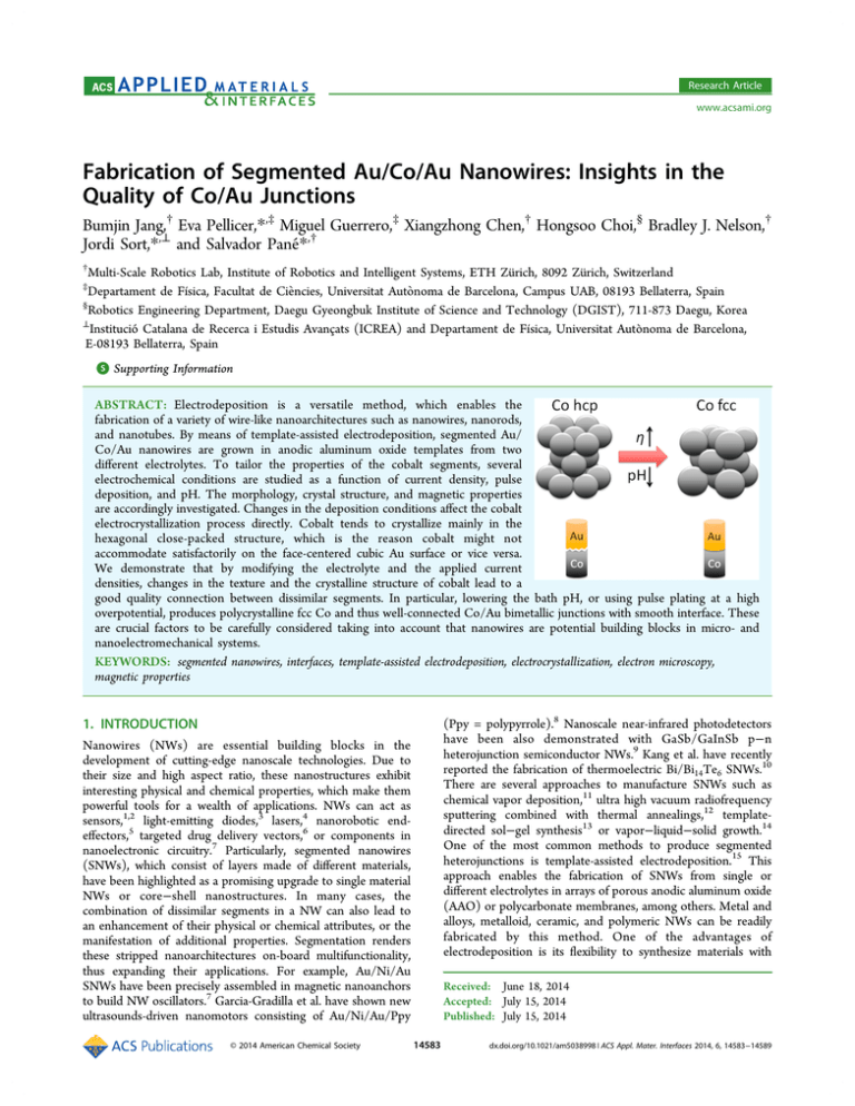
Research Article www.acsami.org Fabrication of Segmented Au/Co/Au Nanowires: Insights in the Quality of Co/Au Junctions Bumjin Jang,† Eva Pellicer,*,‡ Miguel Guerrero,‡ Xiangzhong Chen,† Hongsoo Choi,§ Bradley J. Nelson,† Jordi Sort,*,⊥ and Salvador Pané*,† † Multi-Scale Robotics Lab, Institute of Robotics and Intelligent Systems, ETH Zürich, 8092 Zürich, Switzerland Departament de Física, Facultat de Ciències, Universitat Autònoma de Barcelona, Campus UAB, 08193 Bellaterra, Spain § Robotics Engineering Department, Daegu Gyeongbuk Institute of Science and Technology (DGIST), 711-873 Daegu, Korea ⊥ Institució Catalana de Recerca i Estudis Avançats (ICREA) and Departament de Física, Universitat Autònoma de Barcelona, E-08193 Bellaterra, Spain ‡ S Supporting Information * ABSTRACT: Electrodeposition is a versatile method, which enables the fabrication of a variety of wire-like nanoarchitectures such as nanowires, nanorods, and nanotubes. By means of template-assisted electrodeposition, segmented Au/ Co/Au nanowires are grown in anodic aluminum oxide templates from two different electrolytes. To tailor the properties of the cobalt segments, several electrochemical conditions are studied as a function of current density, pulse deposition, and pH. The morphology, crystal structure, and magnetic properties are accordingly investigated. Changes in the deposition conditions affect the cobalt electrocrystallization process directly. Cobalt tends to crystallize mainly in the hexagonal close-packed structure, which is the reason cobalt might not accommodate satisfactorily on the face-centered cubic Au surface or vice versa. We demonstrate that by modifying the electrolyte and the applied current densities, changes in the texture and the crystalline structure of cobalt lead to a good quality connection between dissimilar segments. In particular, lowering the bath pH, or using pulse plating at a high overpotential, produces polycrystalline fcc Co and thus well-connected Co/Au bimetallic junctions with smooth interface. These are crucial factors to be carefully considered taking into account that nanowires are potential building blocks in micro- and nanoelectromechanical systems. KEYWORDS: segmented nanowires, interfaces, template-assisted electrodeposition, electrocrystallization, electron microscopy, magnetic properties (Ppy = polypyrrole).8 Nanoscale near-infrared photodetectors have been also demonstrated with GaSb/GaInSb p−n heterojunction semiconductor NWs.9 Kang et al. have recently reported the fabrication of thermoelectric Bi/Bi14Te6 SNWs.10 There are several approaches to manufacture SNWs such as chemical vapor deposition,11 ultra high vacuum radiofrequency sputtering combined with thermal annealings,12 templatedirected sol−gel synthesis13 or vapor−liquid−solid growth.14 One of the most common methods to produce segmented heterojunctions is template-assisted electrodeposition.15 This approach enables the fabrication of SNWs from single or different electrolytes in arrays of porous anodic aluminum oxide (AAO) or polycarbonate membranes, among others. Metal and alloys, metalloid, ceramic, and polymeric NWs can be readily fabricated by this method. One of the advantages of electrodeposition is its flexibility to synthesize materials with 1. INTRODUCTION Nanowires (NWs) are essential building blocks in the development of cutting-edge nanoscale technologies. Due to their size and high aspect ratio, these nanostructures exhibit interesting physical and chemical properties, which make them powerful tools for a wealth of applications. NWs can act as sensors,1,2 light-emitting diodes,3 lasers,4 nanorobotic endeffectors,5 targeted drug delivery vectors,6 or components in nanoelectronic circuitry.7 Particularly, segmented nanowires (SNWs), which consist of layers made of different materials, have been highlighted as a promising upgrade to single material NWs or core−shell nanostructures. In many cases, the combination of dissimilar segments in a NW can also lead to an enhancement of their physical or chemical attributes, or the manifestation of additional properties. Segmentation renders these stripped nanoarchitectures on-board multifunctionality, thus expanding their applications. For example, Au/Ni/Au SNWs have been precisely assembled in magnetic nanoanchors to build NW oscillators.7 Garcia-Gradilla et al. have shown new ultrasounds-driven nanomotors consisting of Au/Ni/Au/Ppy © 2014 American Chemical Society Received: June 18, 2014 Accepted: July 15, 2014 Published: July 15, 2014 14583 dx.doi.org/10.1021/am5038998 | ACS Appl. Mater. Interfaces 2014, 6, 14583−14589 ACS Applied Materials & Interfaces Research Article Scheme 1. Fabrication Process of Au/Co/Au SNWsa a EVAP and EP stand for evaporation and electrodeposition, respectively. plating was performed, two different current densities of jdc = −5 and −60 mA cm−2 were employed at a fixed pH = 5.0 and T = 27 °C (room temperature, RT). A pH = 1.95 was used to investigate the effect of pH. For this experiment, current density and temperature were fixed as jdc = −5 mA cm−2 and T = RT. PP was conducted at jpulse = −40 and −600 mA cm−2 with fixed tpulse = 8 ms, trest = 160 ms, pH = 5.0, and T = RT. During the entire deposition process, a platinum electrode served as the counter electrode and N2 agitation was used to stir the solution. The pH of the Au electrolyte was adjusted using citric acid. H2SO4 and NaOH solutions were used to achieve the desired pH value of Co bath. 2.2. Characterization Methods. Scanning electron microscopy (SEM) and transmission electron microscopy (TEM) images of the SNWs were taken on Zeiss ULTRA 55 and HF3300 Hitachi High Technology microscopes, respectively. X-ray diffraction (XRD) patterns were acquired on an Empyrean ALPHA-1 from Panalytical, using Cu Kα radiation. The room temperature magnetic properties were measured using a vibrating sample magnetometer (VSM) from Oxford Instruments. Hysteresis loops were recorded under a maximum applied field of 1 T applied along the directions parallel and perpendicular to the NWs axis. Both XRD and vibrating sample magnetometry (VSM) analyses were done on the NWs still embedded in the AAO templates. different properties by modifying in a very simple manner the composition of the electrolyte (additives, pH) and/or the electrochemical conditions (temperature, stirring regime, potential or current density or substrate). For example, Searson and co-workers have shown that it is possible to modulate the magnetic properties of Cu/Ni SNWs by changing the segment size and the pore dimensions of the templates.16 However, not all the conditions lead to well-built heterojunctions. For example, Whitesides and co-workers have shown that polyaniline (PANI) segments exhibit poor adhesion to metal segments if a self-assembled monolayer is not introduced so as to enable the adhesion of PANI onto Au and Cu segments.17 Also, if higher overpotentials are applied, then nanotubes are formed,18 thus hindering the subsequent integration of another segments. Here, we report the fabrication of Au/Co/Au NWs by sequential electrodeposition from two different electrolytes. First, Au is electrodeposited from a cyanide-based formulation. Subsequently, Co is deposited using different electrochemical conditions in order to induce changes in its crystalline structure and magnetic properties. Finally, a second segment of Au is electrodeposited on top. Interestingly, we have observed that the internanowire junctions may exhibit some defects usually leading to broken nanostructures. An explanation based on crystallographic considerations is provided. 3. RESULTS AND DISCUSSION The fabrication process of Au/Co/Au SNWs is depicted in Scheme 1. A Au seed layer is first evaporated on the backside of the AAO template. Then, a Au plug layer and a Cu sacrificial layer are electrodeposited subsequently. On top of the Cu sacrificial layer, the Au bottom segment (∼0.5 μm in length), Co body segment (∼5 μm in length), and Au top segment (∼0.5 μm in length) are electroplated subsequently to form Au/Co/Au SNWs. Inserting a Cu sacrificial layer benefits the fabrication process at least in three aspects. First, when the first Au plug layer is deposited, the electrolyte leaks through the unblocked openings of the AAO template causing a higher vertical growth rate than a lateral growth rate. Consequently, the formation of a rough and uneven surface of Au segments can occur, precluding a good adhesion with the Co segments. Second, the nanochannels at the bottom of the AAO templates are branched, and these branches would be filled by the electrodeposited nanostructures. By inserting a sacrificial layer, the branched structures can be isolated from the Au/Co/Au NWs. Third, Au/Co/Au NWs can be easily released from the template by etching AAO template and Cu sacrificial layer simultaneously. If there is no Cu sacrificial layer, the NWs remain connected through the Au plug layer. Figure 1 shows a SEM image of the bottom part of the NWs, for which Cu/Au/ Co segments can be distinguished before Cu is etched away during template removal. It can be seen that the Au and Co 2. EXPERIMENTAL SECTION 2.1. Synthesis of the Au/Co/Au SNWs. Anodic aluminum oxide (AAO) templates with 200 nm pore diameter (Anodisk 47, Whatman) were used for the deposition of Au/Co/Au SNWs. A 350 nm-thick Au layer was sputtered on the filtration side of the AAO template, which served as the working electrode. The AAO template was subsequently mounted on an electrically conductive Cu sheet and clamped by means of a homemade holder. A Cu sacrificial layer was initially electrodeposited from a bath containing copper sulfate pentahydrate (CuSO4·5H20, 200 g L−1) and sulfuric acid (H2SO4, 20 g L−1) at pH 1.27. Electrodeposition was carried out at room temperature at a current density of −2 mA cm−2. Au and Co electrolytes were prepared as follows. The cyanide Au electrolyte was composed of gold(I) potassium cyanide (AuK(CN)2, 8 g L−1), potassium citrate (C6H5K3O7, 90 g L−1), citric acid (C6H8O7, 90 g L−1), and 10 mL L−1 of a brightener concentrate which contained cobalt(II) carbonate as a grain refiner (0.05 g L−1). No Co was detected in pure gold segments. The Co bath contained cobalt(II) sulfate hexahydrate (CoSO4·6H2O, 120 g L−1) and boric acid as a buffer agent (H3BO3, 45 g L−1). The sequence of electrodeposition for the synthesis of SNWs was: Au bottom segment, Co segment and Au top segment. The deposition conditions for the Au segments were held constant for all experiments with jdc = −2 mA cm−2, pH = 3.5, and T = 35 °C. Conditions were varied for cobalt deposition as follows. The effect of current density was investigated using both direct current (DC) plating and pulsed plating (PP) methods. When DC 14584 dx.doi.org/10.1021/am5038998 | ACS Appl. Mater. Interfaces 2014, 6, 14583−14589 ACS Applied Materials & Interfaces Research Article Figure 2. SEM images of the cross-sectional view of top Co/Au interface morphology. The Co segments are DC electroplated at −5 mA cm−2 for 2941 s (a) and −60 mA cm−2 for 172 s (b). Figure 1. SEM image of cross-sectional view of SNWs showing Cu/ Au/Co sequence at the bottom. Deposition times are 1360 s for Cu, 704 s for Au, and 50 min for Co. segments are connected very well, and the interfaces between them are smooth. It is worth to mention that smooth Co/Au interfaces are usually easy to obtain, and the quality of the junctions is not very sensitive to the electroplating conditions such as pH and moderate variations of current densities. The reason may lie in that the fcc (face-centered cubic) Co can grow epitaxially on the fcc Au up to a critical thickness of less than 50 nm.19 The subsequent growth of Co, however, is governed by the applied electrodeposition conditions. Therefore, the resulting microstructure (crystallographic phase, grain size, texture) will inevitably influence the connection of Co with the next deposited Au top segment. Therefore, in the following sections, we focus on how to build good quality Co/Au junctions. A thorough study of the influence of electrodeposition conditions on Co segment structures is provided. 3.1. Effect of Current Density and pH in Direct Current (DC) Deposition. One of the strategies to easily induce changes in the Co crystallographic structure consists of changing the applied current density (or the potential) during deposition.20,21 Herein, we studied how different current densities (−j = 5−60 mA cm−2) affect the Au/Co interface morphology as a result of changes in the crystalline structure of Co segments. Note that current densities more negative than −60 mA cm−2 were not considered in order to avoid the formation of Co nanotubes (Supporting Information Figure S1). The pH of Co bath was fixed to 5.0. Lower pH values were also investigated (Supporting Information Figure S3). Figure 2 shows the Co/Au bimetallic junctions of two representative samples electrodeposited at −5 and −60 mA cm−2, respectively. For each sample, both the Au and Co segments have smooth surfaces over the NW walls. Moreover, there is no obvious difference between the surface morphology of Co segments, although the applied current densities differ greatly. However, cracked and porous interfaces are observed at −5 and −60 mA cm−2, respectively. Considering the smooth surface of individual segments, which indicates that the electroplating conditions are good enough for each segment, we can straightforwardly suppose that the defective interfaces are due to the lattice mismatch between the Au and the Co segments. To verify the hypothesis of lattice mismatch, XRD and selected area electron diffraction (SAED) analyses were carried out and the data are presented in Figure 3. Note that while the XRD patterns were acquired with the SNWs still embedded in Figure 3. (a) XRD patterns of Au/Co/Au SNWs. (b and c) SAED patterns of single Co segments electrodeposited at (b) −5 mA cm−2 and (c) −60 mA cm−2. the AAO template (i.e., oriented vertically), the SAED patterns were acquired on SNWs deposited onto TEM grids (i.e., oriented horizontally). In the sample deposited at −5 mA cm−2 for Co, XRD shows the appearance of three strong peaks (denoted with asterisk) at 2θ = 41.6°, 47.5°, and 75.8° (Figure 3a, see Supporting Information Figure S2 for XRD patterns plotted in q-scale), indexed to Co hcp (100), hcp (101), and hcp (110)/fcc (220), respectively. The strongest peak at 41.6° indicates that hcp (100) plane is the preferred orientation along to the Co segment axis, since, according to the tabulated Powder Diffraction Datafile PCPDF 05-0727, the (101) peak should be the most intense for isotropic hcp-Co. The SAED pattern in Figure 3b indicates that this Co segment consists of polycrystalline hcp Co, in agreement with XRD analysis. A different crystallographic texture is observed for the sample obtained at −60 mA cm−2 (Figure 3a), where the peaks corresponding to Co hcp (100) and (101) are considerably reduced in intensity compared to the sample obtained at −5 mA cm−2. Moreover, higher current densities also promote the formation of a fraction of fcc-Co. The fcc (220) peak appears as a shoulder close to the hcp (100) peak, at around 75.8°. The strong intensity of the fcc (220) suggests that the fcc phase is 14585 dx.doi.org/10.1021/am5038998 | ACS Appl. Mater. Interfaces 2014, 6, 14583−14589 ACS Applied Materials & Interfaces Research Article also textured (PCPDF 15-0806). Accordingly, the SAED pattern (Figure 3c) shows not only spots assigned to the hcp phase, but also some of the fcc phase. It has been reported that the formation of fcc Co, which is actually metastable cobalt hydride (fcc), can be promoted by codeposition of hydrogen.22 When a higher overpotential or current density is applied, the electrolysis of water is enhanced so that high adsorption and subsequent codeposition of hydrogen atoms occur. For this reason, Co segments prepared at −60 mA cm−2 exhibit higher proportion of fcc phase than the ones at −5 mA cm−2. The presence of Co fcc phase leads to a significant improvement in the quality of the Co/Au connections. However, some porosity is still observed at the junctions. On the other hand, the remaining hcp Co phase, which was not observed in other studies,20,21,23 can be interpreted considering the differences in current density distribution within a pore and also between pores of different sizes. The templates used in our study have a nominal pore diameter of 200 nm while the templates employed in other works have pores with diameters less than 50 nm. First, the electric field strength and, in turn the current density, is higher at the edge of the pore than in the center. Moreover, the local current density increases with reducing the pore size. Consequently, the more confined the space where electrodeposition takes place is, the higher the hydrogen evolution is. Since the formation of hydrogen enhances the formation of Co fcc, it is reasonable to accept that at the same electrodeposition conditions, it is easier to obtain Co fcc for smaller pores. Further increase of the current density during DC plating process may favor the formation of Co fcc phase, but unfortunately, in our case, current densities more negative than −60 mA cm−2 lead to nanotubes instead of NWs (Supporting Information Figure S1). One possible strategy to get fcc Co is to decrease the pH of the bath.22,24 Similar to the effect of current densities, the influence of solution pH on the microstructure of Co nanosegments is closely related to the incorporation of foreign substances, i.e., hydrogen during electrodeposition. In the present work, the influence of the bath pH was also examined. As expected, Co electrodeposited at a lower pH (∼1.9) exhibits a higher amount of fcc phase, and thus, the Co/Au interface is rather smooth (Supporting Information Figure S3). The potential at pH 1.9 (−2.2 V) is more negative than that at pH 5.0 (−1.8 V) for a current density of −5 mA cm−2 (Supporting Information Figure S4). The higher overpotential is attributed to the higher adsorption of foreign substances, i.e., hydrogen on the electrode surface.22 Although tuning the pH might be convenient, the use of electrolytes with low pH bath might compromise the chemical stability of AAO templates. Here, we propose PP at high overpotentials as an alternative approach. 3.2. Effect of PP Process. The pH of Co bath for the PP studies is fixed at 5.0, the same as in DC. In the case of DC electroplating, the highest applied current density (−60 mA cm−2) was not enough to yield predominant Co fcc phase over hcp phase due to insufficient hydrogen absorption on the deposition sites. While applying a higher current density leads to hydrogen bubbles trapped inside the nanopore structure during DC plating (thus affecting the growth mechanism of Co NWs25), pulse plating provides rest phases which allow uniform nucleation of Co in the nanopores. As a result, NWs can be produced at current densities as large as −600 mA cm−2. Different current densities ranging from −40 to −600 mA cm−2 were examined and two representative samples (obtained at the two extreme j values) are shown to reveal the effect of the overpotential on the Co microstructure. For the sample prepared at j = −40 mA cm−2, the three peaks at 41.6°, 47.4°, and 76.2° in the XRD pattern are assigned to Co hcp (100), hcp (101), and hcp (110), respectively (Figure 4a, see Supporting Information Figure S2 for XRD patterns Figure 4. (a) XRD patterns of pulse-plated Au/Co/Au SNWs. (b and c) SAED patterns of single Co segments electrodeposited at (b) −40 mA cm−2 and (c) −600 mA cm−2. plotted in q-scale). Interestingly, the SAED pattern shows a periodic pattern (Figure 4b), which indicates that Co segments plated under this condition are single-crystalline hcp phase in the zone close to the gold segment. Probably, the use of a very low duty cycle (1.3%) provides enough time for lattice relaxation at the metal−solution interface, thus leading to highly ordered crystalline hcp phase. On the other hand, for the sample obtained at −600 mA cm−2, the XRD pattern shows almost utterly fcc crystalline structure, as corroborated by the SAED pattern (Figure 4a,c). The strong intensity of fcc (220) diffraction peak indicates that this plane is the preferred orientation along Co segments. The fcc (111) and fcc (200) peaks become clearly visible in the SAED pattern, for which the NWs are placed horizontally onto the TEM grid. The very weak intensity of hcp (100) and (101) is probably due to the partial phase transition from Co-fcc to Co-hcp. Decomposition of metastable Co hydrides by the fast diffusion of hydrogen at RT contributes to this phase transition.22 The measured potential during direct and pulsed current plating reveals that the effect of overpotential would be at least 2.5 times higher for the pulsed current plating; E (PP, j= −600 mA cm−2) = 10 V, whereas E (DC, j = −60 mA cm−2) = 4.5 V (Supporting Information Figure S5). Therefore, the abundant hydrogen generated during the plating is effectively adsorbed and subsequently codeposited with Co to form the fcc phase. On the other hand, the applied rest phase (160 ms) is much longer than the pulsed phase (8 ms), which allows a more homogeneous nucleation within the pore, thus avoiding the formation of nanotubes. Figure 5 presents the large differences between the interfaces of the two samples. As expected, for the sample plated at −40 14586 dx.doi.org/10.1021/am5038998 | ACS Appl. Mater. Interfaces 2014, 6, 14583−14589 ACS Applied Materials & Interfaces Research Article Figure 5. SEM images of the cross-sectional view of top Co/Au interface morphology. The Co segments are pulse-plated at −40 mA cm−2 for 8100 s (a) and −600 mA cm−2 for 540 s (b). mA cm−2 (with hcp phase dominating), a severely cracked interface (Co/Au) was observed. Single-crystalline Co hcp phase causes more severe lattice mismatch with Au segments than polycrystalline hcp phase does. The cracked interface usually leads to the detachment of Au segments, as it can be observed in the TEM images (Supporting Information Figures S6 and S7). In contrast, fcc Co deposited at a much high current density (−600 mA cm−2) exhibits excellent adhesion with the subsequent Au top layer (Figure 5b). The interface morphologies of Au/Co NWs related to Co phases are summarized in Table 1. The Co phase plays an Figure 6. Room-temperature hysteresis loops of Au/Co/Au SNW arrays measured (a) parallel and (b) perpendicular to the NW axis (i..e, axis along the NW) directions. Table 1. Summary of the Interface Morphologies as a Function of Co Microstructure crystallographic structure of Co interface morphology of Co/Au Single crystalline-like hcp phase Polycrystalline hcp phase Coexistence of hcp and fcc phases Polycrystalline fcc phase Severely cracked interface Cracked interface Porous interface Smooth interface noninteracting NWs. Conversely, the NWs investigated in this work exhibit sheared hysteresis loops along both directions of measurement with rather low values of coercivity and remanence-to-saturation magnetization ratio. Such an effect can be ascribed to the competition between the magnetic effective anisotropy (shape and magnetocrystalline anisotropies) and the dipolar fields created between neighboring NWs. For a twodimensional infinite array of cylindrical particles with radius r, length L, volume V = πr2L, and interparticle distance D, the total dipolar field when all particles are oriented along the parallel (∥) direction can be written as29−31 important role in determining the interface morphology. Namely, the junction morphology is improved with an increase in Co fcc phase and a reduction in Co hcp phase. Moreover, the degree of crystallinity of the Co hcp phase affects the level of cracks at the interface significantly. 3.3. Magnetic Properties. Figure 6 shows the roomtemperature hysteresis loops of Au/Co/Au SNW arrays (still embedded in the AAO templates), deposited by DC at −5 mA cm−2 and PP at −600 mA cm−2 that correspond to Co segments consisting of almost pure hcp and fcc, respectively. The response is typical of a soft-ferromagnetic material. Interestingly, the in-plane and out-of-plane coercivity of the SNWs deposited by DC at −5 mA cm−2 is slightly larger because of the greater magnetocrystalline anisotropy of the hexagonal phase.26 The loops are rather sheared both along and perpendicular to the NW axis directions, due to the strong dipolar interactions that take place in such a densely packed array of SNWs.27 Actually, no pronounced differences between the loops measured along and perpendicular to the NW axis are observed. An isolated NW with a large aspect ratio (such as the ones prepared in this study) should exhibit a square hysteresis loop when the magnetic field is applied parallel to the NW axis and a tilted hard-axis loop along the perpendicular (⊥) direction.28 Similar behavior would be expected for an assembly of Hdip,0 ° = 4.2MSV D3 (1) where MS is the saturation magnetization (MS,Co = 1440 emu cm−3). If all moments are aligned perpendicular to the NW direction, then the dipolar field would be Hdip,90 ° = −2.1MSV D3 (2) In turn, the self-demagnetizing field of one NW can be expressed as Hdemag = (N⊥ − N )MS (3) where N⊥ and N∥ are the demagnetizing factors perpendicular to the NW axis and along the axis direction and can be calculated using a prolate spheroid approximation, as follows:32 14587 dx.doi.org/10.1021/am5038998 | ACS Appl. Mater. Interfaces 2014, 6, 14583−14589 ACS Applied Materials & Interfaces Research Article ⎡ Ar 4π ⎢ N = 2 ln(A r + ⎢ A r − 1 ⎣ 2 (A r2 − 1) A r2 ⎤ − 1 ) − 1⎥ ⎥ ⎦ *E-mail: Jordi.Sort@uab.cat. *E-mail: vidalp@ethz.ch. Notes The authors declare no competing financial interest. (4) N⊥ = ■ 4π − N ACKNOWLEDGMENTS Main funding support from the European Community’s Seventh Framework Programme (FP7/2007-2013) under grant agreement 296679 (MANAQA) is acknowledged. E.P., M.G., and J.S. also acknowledge the Spanish Ministerio de Economı ́a y Competitividad (MINECO) (MAT2011-27380C02-01) and the Catalan Government (2014-SGR-1015). E.P. is grateful to MINECO for the ‘Ramón y Cajal’ contract (RYC2012-10839). H.C. acknowledges the MIREBraiN project. (5) 2 Assuming that r ≈ 110 nm and L ≈ 5 μm, eqs 4 and 5 give: N⊥= 6.0200 and N∥= 0.5263. Taking into consideration these assumptions, the total effective anisotropy field can be written as HK,eff = (N⊥ − N )MS − 6.3MSπr 2L D3 + Hmc (6) ■ Here Hmc = 2Kmc/MS is the magnetocrystalline anisotropy contribution, which, in a first approximation, can be considered to be small (magnetocrystalline anisotropy, Kmc, of the order of 5 × 10⁵ erg cm−3, bearing in mind the polycrystalline character of the NWS and the mixture of fcc and hcp phases). Equation 6 predicts that if HK,eff is positive, the magnetic easy axis will be parallel to the NW axis; conversely, for negative HK,eff values, the magnetic easy axis tends to lie perpendicular to the NW axis direction.30 Since the shape of the hysteresis loops measured along the ⊥ and ∥ directions is very similar (Figure 6), it can be assumed that HK,eff ≈ 0. Using eq 6 and the average volume of the synthesized Co segments, an interwire distance D ≈ 550 nm is obtained, which is not far from the average interwire distance determined from SEM (350−400 nm). Actually, eqs 1 and 2 are strictly valid only for ordered square arrays of cylindrical dots.29 Here, the NWs are disposed randomly inside the pores of the AAO templates. It has been reported that such geometrical disorder tends to induce further shearing of the hysteresis loops and an increase of the saturation field.33 Hence, the disordered character of the NWs array may account for the slight discrepancy between the estimated D value and the actual interwire distance determined from SEM imaging. (1) Hernandez-Ramirez, F.; Prades, J. D.; Tarancon, A.; Barth, S.; Casals, O.; Jimenez-Diaz, R.; Pellicer, E.; Rodriguez, J.; Morante, J. R.; Juli, M. A.; Mathur, S.; Romano-Rodriguez, A. Insight into the Role of Oxygen Diffusion in the Sensing Mechanisms of SnO2 Nanowires. Adv. Funct. Mater. 2008, 18, 2990−2994. (2) Choi, K. J.; Jang, H. W. One-Dimensional Oxide Nanostructures as Gas-Sensing Materials: Review and Issues. Sensors 2010, 10, 4083− 4099. (3) Tian, B.; Zheng, X.; Kempa, T. J.; Fang, Y.; Yu, N.; Yu, G.; Huang, J.; Lieber, C. M. Coaxial Silicon Nanowires as Solar Cells and Nanoelectronic Power Sources. Nature 2007, 449, 885−889. (4) Duan, X.; Huang, Y.; Agarwal, R.; Lieber, C. M. Single-Nanowire Electrically Driven Lasers. Nature 2003, 421, 241−245. (5) Fournier-Bidoz, S.; Arsenault, A. C.; Manners, I.; Ozin, G. A. Synthetic Self-propelled Nanorotors. Chem. Commun. 2005, 441−443. (6) Salem, A. K.; Searson, P. C.; Leong, K. W. Multifunctional Nanorods for Gene Delivery. Nat. Mater. 2003, 2, 668−671. (7) Kim, K.; Zhu, F.; Fan, D. L. Innovative Mechanism for Precision Assembling and Actuation of Arrays of Nanowire Oscillators. ACS Nano 2013, 7, 3476−3483. (8) Garcia-Gradilla, V.; Orozco, J.; Sattayasamitsathit, S.; Soto, F.; Kuralay, F.; Pourazary, A.; Katzenberg, A.; Gao, W.; Shen, Y.; Wang, J. Functionalized Ultrasound-Propelled Magnetically Guided Nanomotors: Toward Practical Biomedical Applications. ACS Nano 2013, 7, 9232−9240. (9) Ma, L.; Hu, W.; Zhang, Q.; Ren, P.; Zhuang, X.; Zhou, H.; Xu, J.; Li, H.; Shan, Z.; Wang, X.; Liao, L.; Xu, H. Q.; Pan, A. RoomTemperature Near-Infrared Photodetectors Based on Single Heterojunction Nanowires. Nano Lett. 2014, 14, 694−698. (10) Kang, J.; Shim, W.; Lee, S.; Roh, J. W.; Noh, J.-S.; Voorhees, P. W.; Lee, W. Thermodynamic-Enabled Synthesis of Bi/Bi14Te6 Axial Heterostructure Nanowires. J. Mater. Chem. A 2013, 1, 2395−2400. (11) He, M.; Minus, I.; Zhou, P.; Mohammed, S. N.; Halpern, J. B.; Jacobs, R.; Sarney, W. L.; Salamanca-Riba, L.; Vispute, R. D. Growth of Large-Scale GaN Nanowires and Tubes by Direct Reaction of Ga with NH3. Appl. Phys. Lett. 2000, 77, 3731−3733. (12) Shim, W.; Ham, J.; Lee, K.-I.; Jeung, W. Y.; Johnson, M.; Lee, W. On-Film Formation of Bi Nanowires with Extraordinary Electron Mobility. Nano Lett. 2009, 9, 18−22. (13) Kovtyukhova, N. I.; Mallouk, T. E.; Mayer, T. S. Templated Surface Sol−Gel Synthesis of SiO2 Nanotubes and SiO2-Insulated Metal Nanowires. Adv. Mater. 2003, 15, 780−785. (14) Gudiksen, M. S.; Lauhon, L. J.; Wang, J.; Smith, D. C.; Lieber, C. M. Growth of Nanowire Superlattice Structures for Nanoscale Photonics and Electronics. Nature 2002, 415, 617−620. (15) Nicewarner-Pena, S. R.; Freeman, R. G.; Reiss, B. D.; He, L.; Pena, D. J.; Walton, I. D.; Cromer, R.; Keating, C. D.; Natan, M. J. Submicrometer Metallic Barcodes. Science 2001, 294, 137−141. (16) Chen, M.; Chien, C.-L.; Searson, P. C. Potential Modulated Multilayer Deposition of Multisegment Cu/Ni Nanowires with Tunable Magnetic Properties. Chem. Mater. 2006, 18, 1595−1601. 4. CONCLUSIONS Au/Co/Au SNWs can be obtained through electrodeposition in AAO templates. The growth of second Au segments on Co is crucial to successfully build the SNWs. It is observed that fcc Co favors good connection between the ferromagnetic segment and the subsequent Au layer. The crystallographic phase of Co can be controlled by varying the electroplating conditions. Lowering the bath pH, or using PP at a high overpotential, produces polycrystalline fcc Co and thus well-connected Co/ Au bimetallic junctions with smooth interface. These findings will benefit integration of SNWs as building blocks in microand nanoelectromechanical systems. ■ ASSOCIATED CONTENT ■ AUTHOR INFORMATION REFERENCES S Supporting Information * SEM images of Co nanotubes prepared by DC at −80 mA cm−2; XRD patterns plotted in q-scale; XRD, SAED, and SEM images of Co nanowires prepared by DC at pH = 1.9; potential versus time curves; TEM images of Co/Au interfaces for Co segments deposited by PP at −40 mA cm−2. This material is available free of charge via the Internet at http://pubs.acs.org. Corresponding Authors *E-mail: Eva.Pellicer@uab.cat. 14588 dx.doi.org/10.1021/am5038998 | ACS Appl. Mater. Interfaces 2014, 6, 14583−14589 ACS Applied Materials & Interfaces Research Article (17) Lahav, M.; Weiss, E. A.; Xu, Q.; Whitesides, G. M. Core-Shell and Segmented Polymer-Metal Composite Nanostructures. Nano Lett. 2006, 6, 2166−2171. (18) Narayanan, T. N.; Shaijumon, M. M.; Ajayan, P. M.; Anantharaman, M. R. Synthesis of High Coercivity Cobalt Nanotubes Using Acetate Precursors and Elucidation of Mechanism of Growth. J. Phys. Chem. C 2008, 112, 14281−14285. (19) Wright, J. G. The F.C.C.-H.C.P. Phase Transition in Electrolytically Deposited Epitaxial Cobalt Films. Thin Solid Films 1974, 22, 197−201. (20) Fan, X.-X.; Hu, H.-N.; Zhou, S.-M.; Yang, M.; Du, J.; Shi, Z. Abnormal Temperature Dependence of Coercivity in Cobalt Nanowires. Chin. Phys. Lett. 2012, 29, 077802. (21) Cohen-Hyams, T.; Kaplan, W. D.; Yahalom, J. Structure of Electrodeposited Cobalt. Electrochem. Solid-State Lett. 2002, 5, C75− C78. (22) Nakahara, S.; Mahajan, S. The Influence of Solution pH on Microstructure of Electrodeposited Cobalt. J. Electrochem. Soc. 1980, 127, 283−288. (23) Cortés, A.; Lavín, R.; Denardin, J. C.; Marotti, R. E.; Dalchiele, E. A.; Valdivia, P.; Gómez, H. Template Assisted Electrochemical Growth of Cobalt Nanowires: Influence of Deposition Conditions on Structural, Optical and Magnetic properties. J. Nanosci. Nanotechnol. 2011, 11, 3899−3910. (24) Li, F.; Wang, T.; Ren, L.; Sun, J. Structure and Magnetic Properties of Co Nanowires in Self-Assembled Arrays. J. Phys: Condens. Matter 2004, 16, 8053−8060. (25) Chowdhury, T.; Casey, D. P.; Rohan, J. F. Additive Influence on Cu Nanotube Electrodeposition in Anodised Aluminium Oxide Templates. Electrochem. Commun. 2009, 11, 1203−1206. (26) Sort, J.; Suriñach, S.; Muñoz, J. S.; Baró, M. D.; Wojcik, M.; Jedryka, E.; Nadolski, S.; Sheludko, N.; Nogués, J. Role of Stacking Faults in the Structural and Magnetic Properties of Ball-Milled Cobalt. Phys. Rev. B 2003, 68, 014421. (27) Zeeshan, M. A.; Shou, K.; Pané, S.; Pellicer, E.; Sort, J.; Sivaraman, K. M.; Baró, M. D.; Nelson, B. J. Structural and Magnetic Characterization of Batch-Fabricated Nickel Encapsulated MultiWalled Carbon Nanotubes. Nanotechnology 2011, 22, 275713. (28) Sellmyer, D. J.; Zheng, M.; Skomski, R. Magnetism of Fe, Co and Ni Nanowires in Self-Assembled Arrays. J. Phys.: Condens. Matter 2001, 13, R433−R460. (29) Grimsditch, M.; Jaccard, Y.; Schuller, I. K. Magnetic Anisotropies in Dot Arrays: Shape Anisotropy Versus Coupling. Phys. Rev. B 1998, 58, 11539−11543. (30) Han, G. C.; Zong, B. Y.; Luo, P.; Wu, Y. H. Angular Dependence of the Coercivity and Remanence of Electrodeposited Nano-Wire. J. Appl. Phys. 2003, 93, 9202−9207. (31) Rivas, J.; Bantu, A. K. M.; Zaragoza, G.; Blanco, M. C.; LópezQuintela, M. A. Preparation and Magnetic Behavior of Arrays of Electrodeposited Co Nanowires. J. Magn. Magn. Mater. 2002, 249, 220−227. (32) Vázquez, M.; Vivas, L. G. Magnetization Reversal in Co-Base Nanowire Arrays. Phys. Status Solidi B 2011, 248, 2368−2381. (33) Vázquez, M.; Nielsch, K.; Vargas, P.; Velázquez, J.; Navas, D.; Pirota, K.; Hernández-Velez, M.; Vogel, E.; Cartes, J.; Wehrspohn, R. B.; Gosele, U. Modelling Hysteresis of Interacting Nanowires Arrays. Physica B 2004, 343, 395−402. 14589 dx.doi.org/10.1021/am5038998 | ACS Appl. Mater. Interfaces 2014, 6, 14583−14589
