FIELD PROGRAMMABLE GATE ARRAYS (FPGA)
advertisement
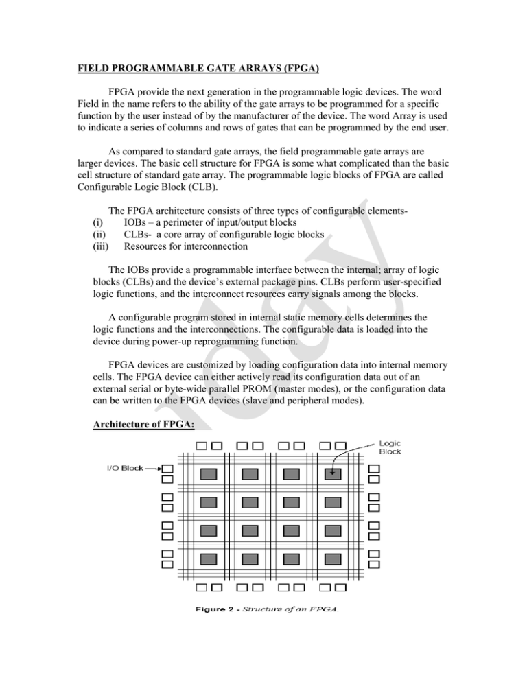
FIELD PROGRAMMABLE GATE ARRAYS (FPGA) FPGA provide the next generation in the programmable logic devices. The word Field in the name refers to the ability of the gate arrays to be programmed for a specific function by the user instead of by the manufacturer of the device. The word Array is used to indicate a series of columns and rows of gates that can be programmed by the end user. As compared to standard gate arrays, the field programmable gate arrays are larger devices. The basic cell structure for FPGA is some what complicated than the basic cell structure of standard gate array. The programmable logic blocks of FPGA are called Configurable Logic Block (CLB). The FPGA architecture consists of three types of configurable elements(i) IOBs – a perimeter of input/output blocks (ii) CLBs- a core array of configurable logic blocks (iii) Resources for interconnection The IOBs provide a programmable interface between the internal; array of logic blocks (CLBs) and the device’s external package pins. CLBs perform user-specified logic functions, and the interconnect resources carry signals among the blocks. A configurable program stored in internal static memory cells determines the logic functions and the interconnections. The configurable data is loaded into the device during power-up reprogramming function. FPGA devices are customized by loading configuration data into internal memory cells. The FPGA device can either actively read its configuration data out of an external serial or byte-wide parallel PROM (master modes), or the configuration data can be written to the FPGA devices (slave and peripheral modes). Architecture of FPGA: The fig .1 shows the general structure of FPGA chip. It consists of a large number of programmable logic blocks surrounded by programmable I/O block. The programmable logic blocks of FPGA are smaller and less capable than a PLD, but an FPGA chip contains a lot more logic blocks to make it more capable. As shown in fig.1 the logic blocks are distributed across the entire chip. These logic blocks can be interconnected with programmable inter connections. Xilinx, Inc inverted FPGAs, and in this section we will see the FPGA architecture used by Xilinx. The programmable logic blocks inn the Xilinx family of FPGAs are called Configurable Logic Blocks (CLBs).The Xilinx architecture uses, CLBs, I/O blocks switch matrix and an external memory chip to realize a logic function. It uses external memory to store the interconnection information. Therefore, the device can be reprogrammed by simply changing the configuration data stored in the memory. Configurable Logic Block: The above figure the logic functions contained within the Xilinx 3000 series configurable logic block. It consists of a combinational logic array, program controlled data multiplexers, and flip-flops. The CLB contains RAM memory cells and can be programmed to realize any function of five variables or any two functions of four variables. The functions are stored in the truth table form, so the number of gates required to realize the functions is not important. In the above fig each trapezoidal block represents a multiplexer, which can be programmed to select one of its inputs. The following fig shows the three different modes of operation for this block (i)FG mode,(ii)F mode,(iii)FGM mode FG Mode: The FG mode generates two functions of four variables each. One variable (A) must be common to both functions. The next two variables can be chosen from B, C, QX and QY. The remaining variable can be either D or E. F Mode: The F mode can generate one function of five variables (A, D, E, and two variables chosen from B, C, QX and QY). FGM Mode: The FGM mode uses a multiplexer with E as a control input to select one of two fourvariable functions. Each function inputs A, D and two of the inputs B, C, QX, QY. The FGM mode can realize the functions of six or seven variables. Cascading of CLBs When we have to implement Boolean function of more than five variables using Xilinx 3000 series then we have to cascade CLBs. The above fig shows the cascading of CLBs. Here two CLBs are used to gate the two intermediate functions of five variables each, then a third CLB is used to gate the two intermediate outputs plus an additional three input variables. Therefore, there are in all 13 variables. Programmable Interconnect: The programmable interconnections between the configurable logic blocks and I/O blocks can be made in several ways (i)General purpose interconnects (ii)Direct interconnect (iii)Vertical & Horizontal Long Line interconnect (i)General purposes interconnect: In general purposes interconnect system, the signals between CLBs or between CLBs and IOBs can be routed through switch matrices as they travel along the horizontal and vertical lines. (ii)Direct Interconnect: Direct interconnection of adjacent CLBs is possible shown in below fig. Long lines are provided to connect CLBs that are far apart. All the interconnections are programmed by storing bits in internal configuration memory cells within the LCA. Long lines provide for high fan-out, low-skew distribution of signals that must travel a relatively long distance. (iii)Vertical & Horizontal Long Line interconnect In the below fig shows there are four vertical long lines between each pair of adjacent columns of CLBs, and two of these can be used for clocks. There are two horizontal long lines between each pair of adjacent rows of CLBs. The long line spans the entire length or width of the interconnection area.
