Bourns Transient Blocking Units
advertisement
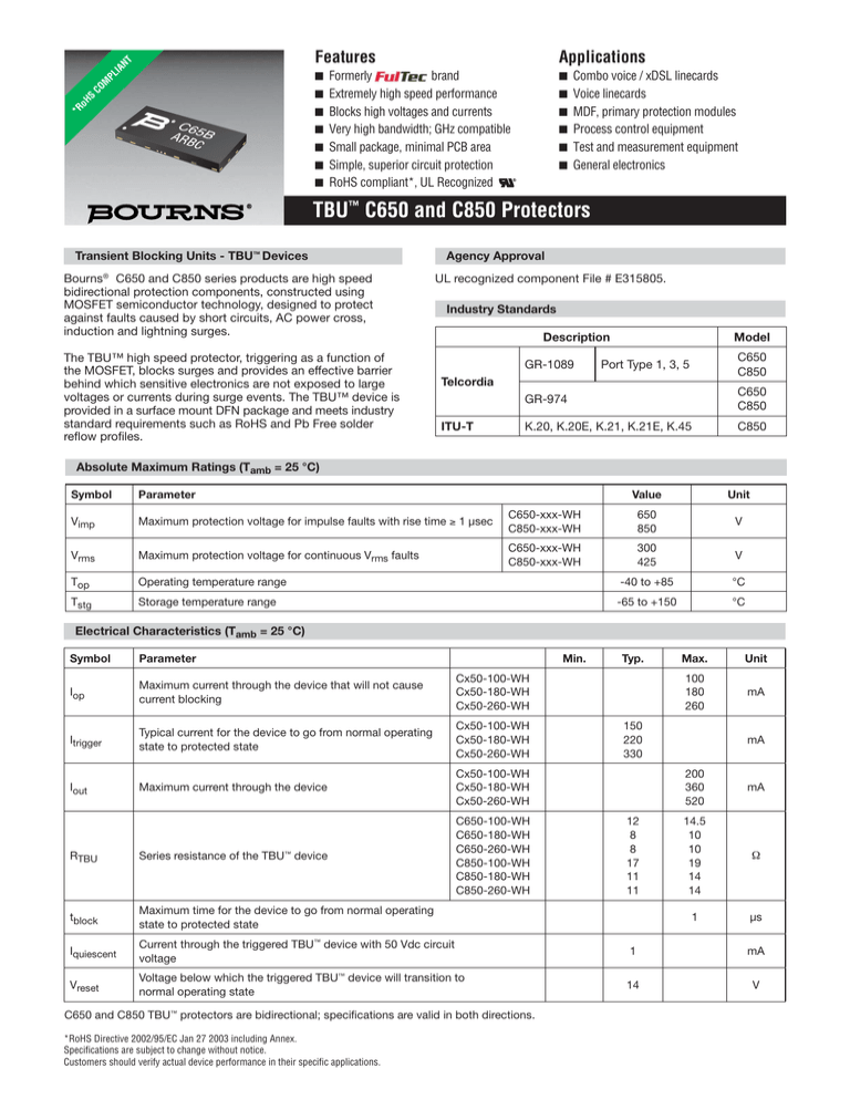
PL IA NT CO M *R oH S Features Applications ■ Formerly ■ Combo voice / xDSL linecards ■ ■ Voice linecards ■ ■ ■ ■ ■ brand Extremely high speed performance Blocks high voltages and currents Very high bandwidth; GHz compatible Small package, minimal PCB area Simple, superior circuit protection RoHS compliant*, UL Recognized ■ MDF, primary protection modules ■ Process control equipment ■ Test and measurement equipment ■ General electronics TBU™ C650 and C850 Protectors Transient Blocking Units - TBU™ Devices Bourns® C650 and C850 series products are high speed bidirectional protection components, constructed using MOSFET semiconductor technology, designed to protect against faults caused by short circuits, AC power cross, induction and lightning surges. The TBU™ high speed protector, triggering as a function of the MOSFET, blocks surges and provides an effective barrier behind which sensitive electronics are not exposed to large voltages or currents during surge events. The TBU™ device is provided in a surface mount DFN package and meets industry standard requirements such as RoHS and Pb Free solder reflow profiles. Agency Approval UL recognized component File # E315805. Industry Standards Description GR-1089 Model C650 C850 Port Type 1, 3, 5 Telcordia ITU-T GR-974 C650 C850 K.20, K.20E, K.21, K.21E, K.45 C850 Absolute Maximum Ratings (Tamb = 25 °C) Symbol Parameter Value Unit Vimp Maximum protection voltage for impulse faults with rise time ≥ 1 µsec C650-xxx-WH C850-xxx-WH 650 850 V Vrms Maximum protection voltage for continuous Vrms faults C650-xxx-WH C850-xxx-WH 300 425 V Top Operating temperature range -40 to +85 °C Tstg Storage temperature range -65 to +150 °C Electrical Characteristics (Tamb = 25 °C) Symbol Parameter Min. Typ. Max. Unit 100 180 260 mA Iop Maximum current through the device that will not cause current blocking Cx50-100-WH Cx50-180-WH Cx50-260-WH Itrigger Typical current for the device to go from normal operating state to protected state Cx50-100-WH Cx50-180-WH Cx50-260-WH Iout Maximum current through the device Cx50-100-WH Cx50-180-WH Cx50-260-WH RTBU Series resistance of the TBU™ device C650-100-WH C650-180-WH C650-260-WH C850-100-WH C850-180-WH C850-260-WH tblock Maximum time for the device to go from normal operating state to protected state Iquiescent Current through the triggered TBU™ device with 50 Vdc circuit voltage 1 mA Vreset Voltage below which the triggered TBU™ device will transition to normal operating state 14 V C650 and C850 TBU™ protectors are bidirectional; specifications are valid in both directions. *RoHS Directive 2002/95/EC Jan 27 2003 including Annex. Specifications are subject to change without notice. Customers should verify actual device performance in their specific applications. 150 220 330 12 8 8 17 11 11 mA 200 360 520 mA 14.5 10 10 19 14 14 Ω 1 µs TBU™ C650 and C850 Protectors Typical Performance Characteristics Time to Block vs. Fault Current V-I Characteristics 1 +I Itrigger -Vreset +V Vreset Time to Block (sec) 0.1 0.01 0.001 0.0001 0.00001 0.000001 0.0000001 0.1 1 10 100 1000 Fault Current (A ) -Itrigger Current vs. Temperature 140 % of Current 120 100 80 60 40 20 -40 -20 0 20 40 60 80 Temperature (°C) Specifications are subject to change without notice. Customers should verify actual device performance in their specific applications. TBU™ C650 and C850 Protectors Operational Characteristics The graphs below demonstrate the operational characteristics of the TBU™ protector. For each graph the fault voltage, protected side voltage, and current is presented. V2 V1 TEST CONFIGURATION DIAGRAM C650 Lightning, 650 V Load C850 Lightning, 850 V 400 mA/div. 2 3 100 V/div. 400 mA/div. 100 V/div. 3 2 1 1 1 µs/div. Ch1 V1 Ch2 V2 Ch1 V1 Ch3 Current C650 Power Fault, 300 Vrms, 100 A 1 µs/div. Ch2 V2 Ch3 Current C850 Power Fault, 425 Vrms, 100 A 3 3 2 200 mA/div. 100 V/div. 100 V/div. 200 mA/div. 2 1 1 4 ms/div. 4 ms/div. Ch1 V1 Ch2 V2 Ch3 Current Specifications are subject to change without notice. Customers should verify actual device performance in their specific applications. Ch1 V1 Ch2 V2 Ch3 Current TBU™ C650 and C850 Protectors Product Dimensions K B Dim. K J J E C E F 3 2 N A B 1 A C H D PIN 1 D TOP VIEW N SIDE VIEW BOTTOM VIEW F H Recommended Pad Layout 0.70 (.028) 1.15 (.045) J Pad Designation Pad # Apply 1 In/Out 2 NC 3 In/Out 2.625 (.103) 3.55 (.140) E K N Min. Typ. Max. 3.90 (.154) 8.15 (.321) 0.80 (.031) 0.000 (.000) 2.55 (.100) 1.10 (.043) 3.45 (.136) 0.20 (.008) 0.65 (.026) 0.20 (.008) 4.00 (.157) 8.25 (.325) 0.85 (.033) 0.025 (.001) 2.60 (.102) 1.15 (.045) 3.50 (.138) 0.25 (.010) 0.70 (.028) 0.25 (.010) 4.10 (.161) 8.35 (.329) 0.90 (.035) 0.050 (.002) 2.65 (.104) 1.20 (.047) 3.55 (.140) 0.30 (.012) 0.75 (.030) 0.30 (.012) DIMENSIONS: MM (INCHES) NC = Solder to PCB; do not make electrical connection, do not connect to ground. TBU™ protectors have matte-tin termination finish. Suggested layout should use non-solder mask define (NSMD). Recommended stencil thickness is 0.10-0.12 mm (.004-.005 in.) with stencil opening size 0.025 mm (.0010 in.) less than the device pad size. As when heat sinking any power device, it is recommended that, wherever possible, extra PCB copper area is allowed. For minimum parasitic capacitance, do not allow any signal, ground or power signals beneath any of the pads of the device. Thermal Resistances Symbol Rth(j-a) Parameter Junction to leads (package) Value Unit 116 °C/W Reflow Profile Profile Feature Pb-Free Assembly Average Ramp-Up Rate (Tsmax to Tp) 3 °C/sec. max. Preheat - Temperature Min. (Tsmin) - Temperature Max. (Tsmax) - Time (tsmin to tsmax) 150 °C 200 °C 60-180 sec. Time maintained above: - Temperature (TL) - Time (tL) 217 °C 60-150 sec. Peak/Classification Temperature (Tp) 260 °C Time within 5 °C of Actual Peak Temp. (tp) 20-40 sec. Ramp-Down Rate 6 °C/sec. max. Time 25 °C to Peak Temperature 8 min. max. Specifications are subject to change without notice. Customers should verify actual device performance in their specific applications. TBU™ C650 and C850 Protectors How to Order Typical Part Marking C 650 - 180 - WH MANUFACTURER’S TRADEMARK* MARKING NUMBER C65A = C650-100-WH C65B = C650-180-WH C65C = C650-260-WH C85A = C850-100-WH C85B = C850-180-WH C85C = C850-260-WH Form Factor C = One TBU™ protector in the device Impulse Voltage Rating 650 = 650 V 850 = 850 V Iop Indicator 100 = 100 mA 180 = 180 mA 260 = 260 mA PIN 1 MANUFACTURING DATE CODE* - 1ST DIGIT INDICATES THE YEAR’S 6-MONTH PERIOD. - 2ND DIGIT INDICATES THE WEEK NUMBER IN THE 6-MONTH PERIOD. - 3RD & 4TH DIGITS INDICATE SPECIFIC LOT FOR THE WEEK. 6-MONTH PERIOD CODES: A = JAN-JUN 2009 C = JAN-JUN 2010 B = JUL-DEC 2009 D = JUL-DEC 2010 E = JAN-JUN 2011 F = JUL-DEC 2011 EXAMPLE: ARBC - 1ST DIGIT ‘A’ = JAN-JUN 2009 - 2ND DIGIT ‘R’ = WEEK 18; WEEK OF APRIL 27 - 3RD & 4TH DIGITS ‘BC’ = LOT SPECIFIC INFORMATION *TRANSITION FROM FULTEC TRADEMARK AND LOT CODE TO BOURNS TRADEMARK AND DATE CODE IN 2009. Packaging Specifications (per EIA468-B) P0 E D t B P2 TOP COVER TAPE A N F W C D B0 K0 CENTER LINES OF CAVITY A0 P D1 EMBOSSMENT G (MEASURED AT HUB) USER DIRECTION OF FEED QUANTITY: 3000 PIECES PER REEL A Device Min. 326 (12.835) C650, C850 Device C650, C850 Device C650, C850 A0 Min. 4.2 (.165) Min. 1.5 (.059) B0 Max. 4.4 (.173) Min. 8.45 (.333) Max. 1.3 (.051) Min. 7.9 (.311) K0 Min. 1.1 (.043) B Max. 330.25 (13.002) C Max. 2.5 (.098) Min. 12.8 (.504) Max. 1.6 (.063) Min. 1.5 (.059) Max. 4.1 (.161) Min. 1.9 (.075) D Max. 8.65 (.341) Min. 1.5 (.059) Max. 8.1 (.319) Min. 3.9 (.159) P D Max. 13.5 (.531) Min. 20.2 (.795) Max. Min. 1.65 (.065) D1 P0 Max. - G Ref. 16.5 (.650) N Ref. 102 (4.016) E - P2 F Max. 1.85 (.073) Min. 7.4 (.291) Max. 0.35 (.014) Min. 15.7 (.618) t Max. 2.1 (.083) Min. 0.25 (.010) max. 7.6 (.299) W DIMENSIONS: Specifications are subject to change without notice. Customers should verify actual device performance in their specific applications. Max. 16.3 (.642) MM (INCHES) TBU™ C650 and C850 Protectors Reference Application The C-series devices are general use protectors used in a wide variety of applications. The following diagram is one common configuration example of C-series device placement. A cost-effective protection solution combines Bourns® TBU™ protection devices with a pair of MOVs or Bourns® GDTs. The figure below demonstrates the operational characteristics of the circuit. V2 V1 Line OVP TBU™ Device Equip. OVP Line TBU™ Device Common Configuration Diagram 200 mA/div. 3 2 1 1 ms/div. Ch1 V1 Ch2 V2 Ch3 Current C850 with G5200AS 4000 V Lightning 10/700 µsec, 150 A Asia-Pacific: Tel: +886-2 2562-4117 • Fax: +886-2 2562-4116 Europe: Tel: +41-41 768 5555 • Fax: +41-41 768 5510 The Americas: Tel: +1-951 781-5500 • Fax: +1-951 781-5700 www.bourns.com REV. 03/10 COPYRIGHT©2008, BOURNS, INC. LITHO IN U.S.A. e 11/08 FU0801 Specifications are subject to change without notice. Customers should verify actual device performance in their specific applications.
