Fundamentals of a new diode clamping multilevel inverter
advertisement

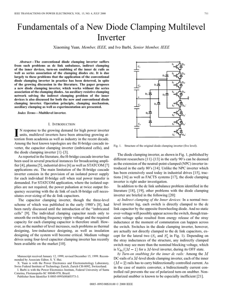
IEEE TRANSACTIONS ON POWER ELECTRONICS, VOL. 15, NO. 4, JULY 2000 711 Fundamentals of a New Diode Clamping Multilevel Inverter Xiaoming Yuan, Member, IEEE, and Ivo Barbi, Senior Member, IEEE Abstract—The conventional diode clamping inverter suffers from such problems as dc link unbalance, indirect clamping of the inner devices, turn-on snubbing of the inner dc rails as well as series association of the clamping diodes etc. It is due largely to these problems that the application of the conventional diode clamping inverter in practice has been deterred, in spite of the growing discussion in the literature. The paper proposes a new diode clamping inverter, which works without the series association of the clamping diodes. An auxiliary resistive clamping network solving the indirect clamping problem of the inner devices is also discussed for both the new and conventional diode clamping inverter. Operation principle, clamping mechanism, auxiliary clamping as well as experimentation are presented. Index Terms—Multilevel inverter. I. INTRODUCTION I N response to the growing demand for high power inverter units, multilevel inverters have been attracting growing attention from academia as well as industry in the recent decade. Among the best known topologies are the H-bridge cascade inverter, the capacitor clamping inverter (imbricated cells), and the diode clamping inverter [1]–[3]. As reported in the literature, the H-bridge cascade inverter has been used in several practical instances for broadcasting amplifier [4], plasma [5], industrial drive [6] as well as STATCOM [7] applications etc. The main limitation of the H-bridge cascade inverter consists in the provision of an isolated power supply for each individual H-bridge cell when real power transfer is demanded. For STATCOM application, where the isolated supplies are not required, the power pulsation at twice output frequency occurring with the dc link of each H-bridge cell necessitates over-sizing of the dc link capacitors. The capacitor clamping inverter, though the three-level scheme of which was published in the early 1980’s [8], had been rarely discussed until the introduction of the “imbricated cells” [9]. The individual clamping capacitor needs only to smooth the switching frequency ripple voltage and the required capacity for each clamping capacitor is therefore small. However, as the number of level increases, such problems as thermal designing, low-inductance designing, as well as insulation designing of the system will become critical. Medium voltage drives using four-level capacitor clamping inverter has recently been available on the market [10]. Manuscript received January 12, 1999; revised December 15, 1999. Recommended by Associate Editor, S. Y. Hui. X. Yuan is with the Power Electronics and Electrometrology Laboratory, Swiss Federal Institute of Technology Zurich, Zurich CH-8092, Switzerland. I. Barbi is with the Power Electronics Institute, Federal University of Santa Catarina, Florianopolis-SC 88040-970, Brazil. Publisher Item Identifier S 0885-8993(00)05573-3. Fig. 1. Structure of the original diode clamping inverter (five level). The diode clamping inverter, as shown in Fig. 1, published by different researchers [11]–[13] in the early 90’s can be deemed as the extension of the neutral-point-clamped (NPC) inverter introduced in the early 80’s [14]. Unlike the NPC inverter which has been extensively used today in industrial drives [15], tractions [16] as well as FACTS systems [17], the diode clamping inverter is right under investigation. In addition to the dc link unbalance problem identified in the literature [18], [19], other problems with the diode clamping inverter are briefed in the following [20]: a) Indirect clamping of the Inner devices: In a normal twolevel inverter leg, each switch is directly clamped to the dc link capacitor by the opposite freewheeling diode. And no static over-voltage will possibly appear across the switch, though transient voltage spike resulted from energy release of the stray inductance at the moment of commutation can happen across the switch. Switches in the diode clamping inverter, however, are actually not directly clamped to the dc link capacitors, exin Fig. 1). Depending on cept for the lateral two ( and the stray inductances of the structure, any indirectly clamped switch may see more than the nominal blocking voltage, which for a -level inverter, during its OFF state. is b) Turn-on snubbing for the inner dc rails: Among the DC-rails of a -level diode clamping inverter, each of the inner rails has to carry bidirectionally controlled current. As in the case of matrix converter, a bidirectionally current controlled rail prevents the use of polarized turn-on snubber. Nonpolarized snubber is known to be especially inefficient [21]. 0885–8993/00$10.00 © 2000 IEEE 712 IEEE TRANSACTIONS ON POWER ELECTRONICS, VOL. 15, NO. 4, JULY 2000 Fig. 2. Structure of the conventional diode clamping inverter with series clamping diodes (five level). c) Multiple blocking voltage of the clamping diodes: Even though each main switch is supposed to block the nominal blocking voltage, the blocking voltage of each clamping diode in the diode clamping inverter is dependent on its position in the structure. For a -level leg, one can find two diodes each sees blocking voltage of Fig. 3. Structure of the proposed new diode clamping inverter (five level). equal voltage rating are used, which are the same with the conventional diode clamping inverter with diodes in series. This pyramid architecture is extensible to any level unless otherwise practically limited. A -level inverter leg requires storage capacitors, switches and clamping diodes. A. Switching Cells and Forward/Freewheeling Paths (1) is the number of levels, goes from 1 to and where is the total dc link voltage. The indirect clamping problem comes inherently with the diode clamping structure of the circuit. Unless an active switch be put in parallel with each clamping diode (which achieves direct clamping), the problem may not be removed. However, the problem will be mitigated when stray inductance is reduced, or when an effective auxiliary clamping is installed. As a result of the turn-on snubbing problem, using of switching devices like GTO’s or IGCT’s in the diode clamping inverter is thought to be a challenging subject. dc rails polarized turn-on snubbers [22] will worsen the static over-voltage problem of the inner devices. As problem (c) is concerned, conventional solution has been to put appropriate number of diodes in series [1], as shown in Fig. 2. The possible over-voltages across the series diodes due to the diversities of diodes switching characteristics as well as their stray parameters call for large RC snubbing network to be introduced leading to expensive and voluminous system. It is therefore the objective of the present paper to propose an alternative diode clamping inverter, in which problem (c) is removed while a solution for problem (a) is also proposed. II. NEW DIODE CLAMPING INVERTER AND ITS OPERATION The new diode clamping inverter is shown in Fig. 3. For the five-level case, a total of eight switches and twelve diodes of The new diode clamping inverter can be decomposed into two-level switching cells as its basic operation units. For the five-level case, one can define (5-1) switching cells as shown in and are always Figs. 4(a), (b), (c) and (d). In cell (a), and work alternatively connecting the inverter ON, while and respectively. Similarly, in cell (b), output to and are always ON, while and work alternatively and 0 respectively. In connecting the inverter output to and are always ON, while and work cell (c), alternatively connecting the inverter output to 0 and respectively. And finally, in cell (d), and are always and work alternatively connecting the inverter ON, while and respectively. output to Each switching cell works actually as a normal two-level inverter, except for that each forward or freewheeling path in the devices rather than only one. Taking cell cell involves (b) as an example, the forward path of the up-arm involves and , whereas the freewheeling path of the up-arm and , connecting the inverter output to involves level for either positive or negative current flow, as shown in Fig. 5(a). Meantime, as shown in Fig. 5(b), the forward path and , whereas the freeof the down-arm involves and , wheeling path of the down-arm involves connecting the inverter output to zero level for either positive or negative current flow. The following rules govern the switching operation of a -level diode clamping inverter: neighboring switches a) At any moment, there must be that are ON. YUAN AND BARBI: FUNDAMENTALS OF A NEW DIODE CLAMPING MULTILEVEL INVERTER Fig. 4. Four switching cells of the proposed new diode clamping inverter. Fig. 5. Forward and freewheeling paths for the up and down arms of cell (b) in the new diode clamping inverter. b) For each two neighboring switches, the outer switch can only be turned on when the inner switch is ON. 713 c) For each two neighboring switches, the inner switch can only be turned off when the outer switch is OFF. 714 IEEE TRANSACTIONS ON POWER ELECTRONICS, VOL. 15, NO. 4, JULY 2000 Fig. 6. Changes of the clamping diodes blocking states in relation with the blocking states of the switchs in the new diode clamping inverter. B. Clamping Diodes Blocking States Clamping diodes change their blocking states as the switches change their states, as shown in Fig. 6. With inverter output connected to a certain level by relevant switches, the involved clamping diodes will block zero voltage whereas the remaining clamping diodes will block zero or the nominal voltage dependent on their positions in the clamping network. As an example, when inverter output is connected to and ON, as shown level zero with switches in Fig. 6(c), the involved clamping diodes including ; and will all block zero voltage. All outside terminals of the arm including and will be of the same potential at zero. Then must block the nominal voltage as its cathode terminal is at whereas must also block nominal voltage as its level . Besides, as and are anode terminal is at level and must block zero voltage. OFF, When inverter output is connected to or , as it may happen, the corresponding clamping YUAN AND BARBI: FUNDAMENTALS OF A NEW DIODE CLAMPING MULTILEVEL INVERTER 715 (a) (b) Fig. 8. Clamping mechanism for the new diode clamping inverter. (a) Clamping mechanism for the down-arm switches. (b) Clamping mechanism for the up-arm switches. Fig. 7. Inverter output voltage synthesizing in association with the blocking states of switches and clamping diodes in the new diode clamping inverter. diodes blocking states can be deducted similarly, as shown by the other diagrams in Fig. 6. To summarize, in the new diode clamping inverter, always follow always follow always follows ; whereas always follow always follow always follows , without regard to the inverter output level. Inverter output voltage synthesizing in association with blocking states of switches and clamping diodes is shown in Fig. 7. Similar mechanism can be witnessed with cell (b), where are directly clamped to , while are indiare directly clamped to rectly clamped to . In cell (c), , while are indirectly clamped to . In cell (d), are directly clamped to , while are indirectly clamped to . Graphical illustration of the clamping mechanism for the new diode clamping inverter is shown in Fig. 8(a) and (b). In summary, for the proposed new diode clamping inverter, not only the switches are clamped, so are the clamping diodes. Among which, the 8 lateral devices ( , and ) are directly clamped, whereas the remaining devices are indirectly clamped, to the corresponding dc link capacitors. B. Indirect Clamping and Blocking Voltage Distribution III. CLAMPING MECHANISM AND AUXILIARY CLAMPING OF THE NEW DIODE CLAMPING INVERTER A. Switch and Diode Clamping Mechanism As the name of the diode clamping inverter implies, any main switch in the string at blocking state must be clamped to a corresponding dc link capacitor via relevant clamping diodes. By which, blocking voltage of the main switch will be constrained to the nominal value. This mechanism in the proposed diode clamping inverter will be discussed below. and are always Referring back to Fig. 4, in cell (a), and are always OFF, and work alON, while and ternatively connecting the inverter output to respectively. Obviously, is directly clamped to by after it’s turn-off, while in series with and is by and after its indirectly clamped to in series with and is indirectly turn-off. Further, by and ; in series with is clamped to by and , while is directly indirectly clamped to by . Suppose that for cell (a), and clamped to each blocks voltage, and each blocks zero and are all clamped to at voltage. Then, when OFF. Among which and are directly clamped and are indirectly clamped. while Indirect clamping will possibly result in unequal voltage distribution among the blocking devices, due mainly to the stray inductances in the structure. In the following text, the commutato will tion process from is indirectly clamped, , , and be considered. As will have to block more than the nominal voltage during the OFF state. and are ON. Upon the rePrior to commutation, leasing of the turn-off signal for , the stray capacitance of will first be charged. Until the voltage across the stray capacireaches , freewheeling diodes tance of and will conduct, leading to demagnetization of the stray in the clamping path, as shown in Fig. 9. The inductance will be absorbed by the stray capacitance trapped energy in together with the stray capacitances of and . of will continue be charged, whereas The stray capacitance of and will be discharged. the stray capacitances of Such over-charging and discharging will not be recovered subsequently, as the discharging path for the stray capacitance of , and the charging path for the stray capacitances of and are both blocked by and . Consequently, will block more than voltage while and together will block less than voltage during the steady and together sees the difference state. Moreover, 716 IEEE TRANSACTIONS ON POWER ELECTRONICS, VOL. 15, NO. 4, JULY 2000 Fig. 9. Stray inductance demagnetization during the commutation process from S ; D ; D and D to D ; D ; D , and D in the new diode clamping inverter. between the blocking voltage of and . Meanwhile, sees plus and sees plus , while sees . Indirect clamping and the subsequent unequal blocking and and voltage distribution problem holds also for , and , together with their relevant clamping diodes in cell (b), cell (c) and cell (d). Due to the fact that the stray capacitance of the neighboring outer switch experiences one more discharging than the inner switch, among the blocking devices, the outer switch will always block less voltage while the inner device will always block more voltage. The center device will always be exposed to the highest voltage stress. Unequal blocking voltage distribution problem arising from indirect clamping exists also with the conventional diode clamping inverter as mentioned in Section I. The severity of this problem is dependent on the stray inductances of the structure. With refined bus-bar designing technique, and in particular, appropriate positioning of an auxiliary clamping, the problem will be mitigated. Fig. 10 shows a resistive auxiliary clamping network for the new diode clamping inverter. A similar network for the conventional diode clamping inverter is given in Fig. 11. The basic principle has been discussed in [23]. IV. EXPERIMENTATION RESULTS A scaled laboratory prototype has been built for verification of the new diode clamping inverter. For the half bridge five-level prototype, four 120 V dc power sources are employed as the dc supplies for the dc link. The series inductor has been added just to make the dc source operational. As the load for the inverter, a 8 mH inductor in series with a 12 resistor are connected between the inverter output and the dc neutral point. Fundamental frequency modulation scheme eliminating the fifth and the sev- Fig. 10. An auxilairy clamping network configuration for the new diode clamping inverter. Trapped energy in L is now absorbed by C as S is turned off. Fig. 11. An auxiliary clamping for the conventional diode clamping inverter. Each auxiliary clamping diode is subject to multiple blocking voltage. enth harmonics is implemented. For the small power prototype, no auxiliary clamping has been installed. Fig. 12(a)–(d) shows the experimental output voltage in relaand respection to the blocking voltages across tively, which clearly demonstrate the operation and clamping of the proposed new diode clamping inverter. The nonrigidity of the individual voltage level has been caused by the inductor in series with the corresponding dc supply. V. CONCLUSION From the analysis and experimentation presented above, the following conclusions are obtained regarding the new diode clamping inverter: YUAN AND BARBI: FUNDAMENTALS OF A NEW DIODE CLAMPING MULTILEVEL INVERTER Fig. 12. Experimental output voltage of the new inverter in relation to the blocking voltages across S nominal blocking voltage. 1) The new diode clamping inverter solves the diodes series problem of the conventional diode clamping inverter. In the new structure, not only the main switches are clamped by the clamping diodes, the clamping diodes are also clamped mutually by themselves. The need for the large RC network dealing with voltage sharing problem among series diodes is removed. 2) The unequal blocking voltage distribution problem resulted from indirect clamping is expected to be mitigated by adding an auxiliary clamping network. Even though the turn-on snubbing problem and the dc link unbalance problem are not resolved, the new diode clamping inverter represents a relevant improvement over the conventional structure and will facilitate the practical application of the diode clamping multilevel inverter in large power conversion area. REFERENCES [1] J. S. Lai and F. Z. Peng, “Multilevel converters—A new breed of power converters,” IEEE Trans. Ind. Applicat., vol. 32, May/June 1996. [2] A. Rufer, “An aid in the teaching of multilevel inverters for high power applications,” in Proc. Rec. IEEE PESC’95, 1995, pp. 347–352. [3] C. Newton and M. Sumner, “Multilevel converters: A real solution to medium high voltage drives?,” Inst. Electron. Eng.—Power Eng. J., pp. 21–26, Feb. 1998. [4] W. Schminke, “High power pulse step modulator for 500 KW short wave and 600 KW medium wave transmitters,” Brown Bovery Rev., vol. 72, no. 5, pp. 235–240, 1985. [5] M. Marchsoni, M. Mazzucchelli, and S. Tenconi, “A nonconventional power converter for plasma stabilization,” IEEE Trans. Power Electron., vol. 5, pp. 212–219, Apr. 1990. [6] P. W. Hammond, “A new approach to enhance power quality for medium voltage AC drives,” IEEE Trans. Ind. Applicat., vol. 33, pp. 202–208, Jan./Feb. 1997. 717 ;S ;S ; and S respectively. Each main switch sees the [7] J. D. Ainsworth, M. Davies, P. J. Fitz, K. E. Owen, and D. R. Trainer, “Static var compensator (STATCOM) based on single phase chain circuit converters,” IEE Proc.—Gener. Transm. Distrib., vol. 145, no. 4, July 1998. [8] T. Maruyama and M. Kumano, “New PWM control for a three-level inverter,” in Proc. Rec. IPEC, 1990, pp. 870–877. [9] T. Meynard and H. Foch, “Multi-Level conversion: High voltage choppers and voltage source inverters,” in Proc. Rec. IEEE PESC, 1992, pp. 397–403. [10] Y. Shakweh and E. Lewis, “Assesment of medium voltage PWM VSI topologies for multi-megewatt variable speed drive applications,” in Proc. Rec. IEEE PESC, 1999, pp. 965–971. [11] J. M. Andrejak and M. Lescure, “High voltage converters promising technological developments,” in Proc. Rec. EPE Conf., 1987, pp. 1.159–1.162. [12] N. S. Choi, J. G. Cho, and G. H. Cho, “A general circuit topology of multilevel inverter,” in Proc. Rec. IEEE PESC, 1991, pp. 96–103. [13] M. Carpita and S. Tenconi, “A novel multilevel structure for voltage source inverter,” in Proc. Rec. EPE Conf., 1991, pp. 1.90–1.94. [14] A. Nabae, I. Takahashi, and A. Akagi, “A new neutral-point clamped PWM inverter,” IEEE Trans. Ind. Applicat., vol. 19, pp. 518–523, Sept./Oct. 1981. [15] H. Stemmler, “High power industrial drives,” Proc. IEEE, vol. 82, pp. 1266–1286, Aug. 1994. [16] A. Steimel, “Electric railway traction in europe,” IEEE Ind. Applicat. Mag., pp. 7–17, Nov./Dec. 1996. [17] B. A. Renz, A. J. F. Heri, A. S. Mehraban, J. P. Kessinger, C. D. Cchauder, L. Gyugyi, L. J. Kovalsky, and A. A. Edris, “World’s First Unified Power Flow Controller on the AEP System,” Tech. Rep., CIGRE Paper 14-107, 1998. [18] F. Z. Peng, J. S. Lai, and J. MeKeever, “A multilevel voltage-source converter system with balanced dc voltages,” in Proc. Rec. IEEE PESC, 1995, pp. 1144–1150. [19] F. Z. Peng and J. S. Lai, “A static var generator using a staircase waveform multilevel voltage source converter,” in Proc. Rec. Power Quality Conf., Sept. 1994, pp. 58–66. [20] X. Yuan, “Soft Switching Techniques for Multilevel Invreters,” Ph.D. thesis, INEP-UFSC, Brazil, May 1998. [21] W. McMurray, “Resonant snubbers with auxiliary switches,” IEEE Trans. Ind. Applicat., vol. 29, pp. 355–362, Mar./Apr. 1993. 718 [22] I. Kim, E. Nho, and B. Bose, “A new snubber circuit for multilevel inverter and converter,” in Proc. Rec. IEEE IAS Annu. Meeting, 1999, pp. 1432–1439. [23] X. Yuan and I. Barbi, “ARCPI resonant snubber for the neutral-pointclamped inverter,” IEEE Trans. Ind. Applicat., vol. 36, pp. 585–595, Mar./Apr. 2000. Xiaoming Yuan (S’97–M’99) received the M.Eng. degree from Zhejiang University, China, and the Ph.D. degree from the Federal University of Santa Catarina, Florianopolis, Brazil, in 1993 and 1998, respectively, both in electrical engineering. He was an Electrical Engineer with Qilu Petrochemical Corporation, China, from 1986 to 1990. He is currently a postdoctoral researcher with the Power Electronics and Electrometrology Laboratory, Swiss Federal Institute of Technology, Zurich, Switzerland, where he is working on flexible-ac-transmission-system (FACTS) devices. Dr. Yuan received the first prize paper award from the Industrial Power Converter Committee, IEEE Industry Applications Society, in 1999. IEEE TRANSACTIONS ON POWER ELECTRONICS, VOL. 15, NO. 4, JULY 2000 Ivo Barbi (M’78–SM’90) was born in Gaspar, Santa Catarina, Brazil, in 1949. He received the B.S. and M.S. degrees in electrical engineering from the Federal University of Santa Catarina, Florianopolis, Brazil, in 1973 and 1976, respectively, and the Dr.Ing. degree from the Institut National Polytechnique de Toulouse, France, in 1979. He founded the Brazilian Power Electronics Society, the Power Electronics Institute, Federal University of Santa Catarina, and created the Brazilian Power Electronics Conference. Currently, he is Professor of the Power Electronics Institute, Federal University of Santa Catarina. Dr. Barbi has been an Associate Editor for the Power Converters Area of the IEEE TRANSACTIONS ON INDUSTRIAL ELECTRONICS since January 1992.


