Chapter 6 Fabrication Technology of Optoelectronic Devices • Introduction
advertisement
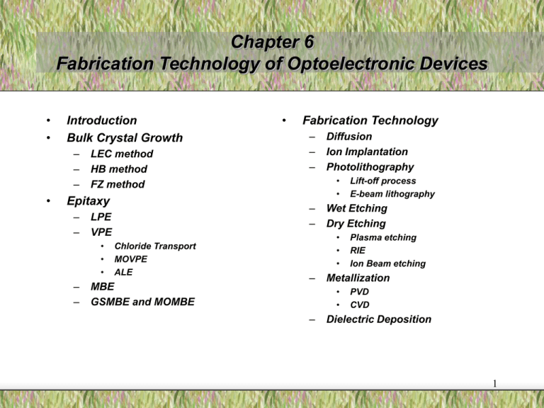
Chapter 6 Fabrication Technology of Optoelectronic Devices • • Introduction Bulk Crystal Growth – – – • LEC method HB method FZ method Epitaxy – – – – Fabrication Technology – – – Chloride Transport MOVPE ALE MBE GSMBE and MOMBE Diffusion Ion Implantation Photolithography • • – – LPE VPE • • • • Wet Etching Dry Etching • • • – Plasma etching RIE Ion Beam etching Metallization • • – Lift-off process E-beam lithography PVD CVD Dielectric Deposition 1 Introduction to Fabrication Process of Optical Devices a) b) c) d) e) * Starting materials → growth of epitaxial layers → deposition of photoresists → deposition of metals → lift-off for formation of top contact Mesa-etching Formation of bottom contact (as in (a)) Mesa-etching for device isolation → deposition of dielectric passivation Overlay metallization for interconnects and bonding pad → deposition of dielectric passivation → substrate thinning and backhole The semi-insulating substrate is used for certain high-speed device (in which both contacts are formed on the top side ), while a conducting substrate is useful for device that has top and bottom contacts. Typical processing for fabricating optoelectronic devices on a semi-insulating substrate 2 Bulk Crystal Growth • Bulk crystal growth technology for III-V compound semiconductors: – – – • Czochralski Crystal Puller Liquid Encapsulated Czochralski (LEC) method Horizontal Bridgmann (HB) method Floating Zone (FZ) method Main reasons for the difference progress between Si and GaAs bulk crystal growth: – – • • The growth of a compound semiconductor is always more difficult than that of a single-element system The demand from device manufacturers for large area compound semiconductors is lacking. (2” or 3” wafers are popularly used in opto-electronic fabrication plants) Synthesis of polycrystalline GaAs as the raw materials to grow single-crystal GaAs: – – – Ga is placed in a graphite boat and heated to 610 to 620 ℃, while As is placed in another graphite boat and heated to 1240 to 1260 ℃ (slight above the melting temperature of GaAs. As is overpressure and will transport to the Ga melt. When the melt cools, a high-quality polycrystalline GaAs results. 3 Liquid Encapsulated Czochralski (LEC) Technology • To prevent decomposition of the melt due during crystal growth due to the high vapor pressure of As, the melt is encapsulated by a layer of boron trioxide. – • • The whole system is contained in a pressure vessel, with an inert gas ambient providing an overpressure (< 3 atm)to the melt. The crucible is pyrolytic boron nitride (PBN), instead of the quartz used in conventional Si CZ method. – – • • B2O3, which is an inert liquid with a low melt point and low vapor pressure. → liquid encapsulant B2O3 can dissolve silicon dioxide (fused-silica) as this material can be used several times over and does not act as a source of intentional silicon dopants. The high dislocation defect density ( 104 to 105 cm-2) produced by this method is its its major its major disadvantage, as compared to the HB method. Semi-insulating wafers are usually made by this method. 4 Horizontal Bridgmann Technology • • • • • The assembly is placed inside a zoned heating system. A GaAs seed crystal is placed at one end of the quartz boat, and molten GaAs is maintained in the bulk of the boat region (T1 zone ~ 1250℃). An arsenic overpressure is provided by the elemental As source in the ampoule. As the seed end of the melt moves out of the T1 zone to the cooler T2 zone, it solidified into single crystal GaAs. The advantages of the HB method over the LEC method: – – • Dislocation densities are usually lower (13104 cm-2) The ability to deliberately incorporate dopants and give a conducting wafer. The disadvantages of the HB method: – – The lack circular wafers of suitable size for IC fabrication. (D-shaped boules are formed.) It can not produce GaP wafers due to the high melting point (1470 ℃ ) of this material. (quartz boat is molten at this point) 5 Floating Zone Technology • The floating zone (FZ) method can be used to grow very purity Si wafers. – • A high-purity polycrystalline rod with a seed crystal at the bottom is held in a vertical position and rotated. – • • • • FZ degree crystal are used mainly for highpower, high-voltage devices, where highresistivity materials are required. The rod is enclosed in a quartz envelope with which an inert gas (Ar) is maintained. During the operation, a small zone of the crystal is kept molten (floating zone) by a RF heater. As the floating zone moves upward, a singlecrystal silicon freezes at the zone’s retreating end and grows as an extension of the seed crystal. Materials with higher resistivities can be obtained from the floating zone process than from the CZ method. Since no crucible is used in this method, there is no contamination from the crucible. 6 Summary of process for GaAs wafer production 7 Epitaxy • • • The word “epitaxy” comes from Greek terms: epi = upon, taxis = arrangement. Bulk crystals can rarely be used for optimized optoelectronic devices for the following reasons: – Light emitters and photodetectors operating at different wavelengths are required. (This requires different semiconductors with different bandgaps.) – Material quality for bulk crystals is generally lower than that of epitaxial layers for compound semiconductors. (However, the reverse is true for silicon.) In the epitaxy process, the wafer (substrate) acts as not only a seed for crystal growth, but also as physical support for the thin epilayer. 8 Liquid Phase Epitaxy (LPE) • • LPE is the growth of epitaxial layers on crystalline substrates by direct precipitation from the liquid phase. (somewhat like the HB method except its more transient growth time) – LPE is the volume method used for standard LED production today. The LPE growth process: – – – – • During operation while the system is heated to the required temperature, the substrate is fully covered by part of the graphite block. When the target temperature is reached, the substrate is moved under te first well and the furnace temperature is lowered at a given rate. To grow additional layers, the substrate can be moved successively under the solution. The wafer is moved out from under the solution to terminate the process. In LPE, the material to be grown must dissolves in a solvent, and the solution must melt at a temperature well below the melting point of the substrate. – Ga is most commonly used as the solvent for the growth of GaAs. 9 Melt-Back LPE Method • • This method was developed primarily for green LEDs based on GaP:S/GaP:Zn junctions. The growth process: A GaP substrate (in contact with a Ga melt) is heated and cooling subsequently to result in an epitaxial layer. Three types of gases are introduced into the hydrogen ambient: – H2S, to provide S doping and result an nlayer. – Zn vapor (from a solid source) to provide a p-layer. – NH3 during junction growth to introduce an isoelectronic center based on nitrogen to maximum the LED efficiency. 10 Vapor Phase Epitaxy (VPE) • • Two types of VPE: (i) Chloride transport (ii) metal-organic VPE (MOVPE) MOVPE, OMVPE (organo-metallic VPE) MOCVD, OMCVD 11 VPE (I) --- Chloride Transport • • Trichloride VPE – In this system, trichloride AsCl3 (or PCl3), which is liquid, is transferred to the reaction chamber by bubbling hydrogen through. – An initial crust of GaAs is formed on the Ga source as a result of the release of arsenic from the incoming gases: 4 AsCl3 + 6 H2 → 12 HCl + As4 Hydride VPE – In this system, hydrides such as arsine (AsH3) and HCl are used. – GaCl is generated from the Ga source and As4 from the pyrolysis of arsine : 2 Ga + 2 HCl → 2 GaCl + H2 4 AsCl3 + 6 H2 → 12 HCl + As4 – GaAs is formed on the substrate by the reaction: GaCl + AsH3 → GaAs + HCl + H2 12 VPE (II) --- MOVPE • In the MOVPE process, the group III compound is transported to the substrate surface in as organic precursor, while arsine (AsH3) or phosgine (PH3) are still used as the carrier for the group V compound. – • • The organic precursors are all liquid at room temperature, so bubbling hydrogen system is used. A reaction occurs near the heated substrate surface to form II-V compound directly from the two carrier gases: (such as) Ga(C2H5)3(g) + AsH3(g) → GaAs(s) + 3 C2H6(g) MOVPE can produce multilayered structures of excellent electrical and morphological characteristics over a large area. Tri-methyl-gallium: Ga(CH3)3 or TMGa Tri-ethyl-gallium: Ga(C2H5)3 or TEGa Tri-ethyl-indium: In(C2H5)3 or TEIn 13 Various MOVPE Systems • Atmospheric-pressure MOVPE – – • Advantage: High growth rate Problems: unwanted polymer formation, autodoping, outdiffusion Low-pressure MOVPE – – • Atmospheric-pressure MOVPE System Eliminating the above problems The main stream of the MOVPE system Photo-MOVPE – – Pyrolytical process Photolytical process 14 Low-Pressure MOVPE 15 Comparison of VPE and LPE • • • • For large scale production of non-critical LEDs, the obvious choice is LPE. The quality of the surface finish of LPE materials is poor. The most important advantage of the VPE over LPE is the ability to grow thin layers of heterostructure material on large area substrates. The competition for the best quality growth technique is really between MOVPE and MBE. 16 Atomic Layer Epitaxy (ALE) • • • The epitaxy process that can deposit atoms one layer at a time. MBE and MOVPE are both the basic ALE systems. The advantages of the ALE process: – Accurate thickness control and reproducibility. – High quality surface finish, free of many types of defects. – The ability to dope selectively grown epitaxial layers – this is useful for heavily doped contact regions. – Sidewall epitaxy, where a previous fabricated multilayer epitaxial wafer can have a different semiconductor grown on the edge, giving threedimensional confinement. 17 Molecular Beam Epitaxy (MBE) • • MBE is an epitaxial process involving the reaction of one or more thermal beams of atoms or molecules with a crystalline surface under ultrahigh vacuum (UHV) conditions (~10-10 Torr). Separate effusion oven (made of pyrolytic boron nitride) are used for Ga, As, and the dopants. – • • The temperature of each oven is adjusted to give the desired evaporation rate. High-temperature baking and low energy ion beam sputter-clean process are used to clean the surface of a substrate in-situ. In-situ analysis includes a mass spectrometer for ‘residual gas analysis’ (RGA) and “reflection high energy electron diffraction” (RHEED) to monitor the substrate and the epilayer quality. 18 Basic Growth Kinetics of MBE 1) 2) 3) • • Evaporation from the source and molecular travel towards the substrate. Absorption onto the substrate. Surface migration and dissociation, leading to incorporation onto the substrate (growth). During MBE process, the substrate temperatures range from 400 to 900℃, and the growth rates range from 0.001 and 0.3 m/min. Because of the low-temperature process and low-growth rate, many unique doping profiles, alloy composition and novel device structures (such as superlattice) not obtainable from conventional VPE and LPE can be produced in MBE. 19 Gas-Source MBE (GSMBE) • The problem with III-V growth using solid source MBE in that the flux of the group V source is much greater that of group III element. – – • • In the GSMBE process, solid source is used for group III material, while hydride gas (AsH3 or PH3) is used as the group V source. During GSMBE, hydride decomposition (AsH3 or PH3 → As2, P2, H2) is achieved by a thermal cracker system. – • Hence, the source is rapid depleted, leading to regular changes. Beam flux variations with time, making it difficult to control. Source supply and control are external to the MBE system, leading a much longer time between source replenishment, and a more easily control flux of group V atoms. The GSMBE has a higher reproducibility than a convention MBE system with solid elemental source. 20 Metal-Organic MBE (MOMBE) • • • In the MOMBE process, gas sources are used for both group III and group V (AsH3 or PH3), with a reaction between TMGa or TEGa (and TMIn or TEIn) on the substrate surface with previous cracked As2 and P2. MOMBE is also known as “chemical beam epitaxy” (CBE). Growth process of MOMBE: – – – • The beam of both gas molecules impinge directly onto the heated substrate surface. The group III alkyl dissociated to leave a free group III atom on the surface and a desorbed alkyl group. Group V elements can then react readily with the surface group III atoms. MOMBE process uses the directional nature of MBE to react gas molecules together (like MOVPE), but only on the substrate surface (unlike MOVPE). 21 Advantages of MOMBE • • Advantages of MOMBE over MBE: – Greater control over a source that will produce many epilayers before needing refurbishment – Reproducibility and the ability to produce very abrupt interface are inherent in this system. – No oval defects (surface defects) – A single group III beam, ensuring composition uniformity Advantages of MOMBE over MOVPE: – The use of RHEED and RGA to monitor epilayer growth and gas stoichiometry in situ. – No flux pattern problems for large area/multi-wafer applications. – More abrupt interfaces due to the beam nature of the growth. 22 Fabrication Technology (1) Doping: Diffusion, Ion Implantation (2) Photolithography: Resist coating, Exposure, Development, Resist removal Lift-off process E-beam lithography (3) Etching: Wet Etching (Isotropic and Anisotropic Etching, Crystallographic) Dry Etching (Plasma etching, RIE, Ion beam etching) (4) Metallization: PVD ( Thermal and E-Beam evaporation, Sputtering) CVD (PECVD, Laser-induced CVD) (5) Dielectric Deposition: PECVD, LPD (Liquid Phase Deposition) 23 Lift-off Process • In the GaAs process, chemical etching is rarely used to pattern metals because: – – • The lift-off technique is capable of high resolution and is used extensively for discrete devices (e.g. high-power MESFET, optoelectronic devices). – • Many metal etchants will also etch GaAs. GaAs processing tends to use multi-layered metals, such as Au/Ge/Ni for n-type (Au/Zn for p-type) ohmic contacts and Ti/Pt/Au for rectifying or overlay metals, which are difficult to etch. However, it is not used as widely applicable for VLSI, in which dry etching is the preferred technique. Lift-off process: – – – (a) & (b) A positive resist is used to form the resist pattern on the substrate. (b) The film is deposited over the resist and the substrate. The film thickness must be smaller than that of the resist. Those portions of the film on the resist are removed by selectively dissolving the resist layer in an appropriate liquid etchant so that the overlying film is lifted off and removed. 24 E-beam lithography • The advantages of E-beam lithography: – • The generation of micron and submicron resist geometries. – Highly automated and precisely controlled operation. – Greater depth of focus (DOF) than that available from optical lithography. – Direct patterning on a wafer without using a mask. – Disadvantage: low throughput Electron Resist: polymers – Positive resist → higher resolution (but slow) PMMA (poly-methyl-methacrylate) PBS (poly-butene-1 sulfone) – Negative resist → higher sensitivity (fast) COP (poly-glycidyl-methacrylate-co-ethyl acrylate) There is a trade-off between sensitivity and resolution. In e-beam lithography, resolution is limited by electron scattering, while is limited by diffraction of light in optical lithography. 25 Wet Etching • • Wet etching → involving chemicals in a liquid solution Dry etching → involving reactive species generated in a plasma Wet chemical etching is used extensively in semiconductor processing: – • • • • • Lapping and polishing of a sawed wafer, chemical cleaning and scrubbing, delineating pattern, opening window. Isotropic etching Anisotropic etching Orientation-dependent etching Crystallographic etching Very few etchants are isotropic for GaAs. – Most etchants give a polished surface on arsenic face, but the gallium face tends to slow crystallographic. 26 Crystallographic Etching • • In diamond and zincblend lattices, the (111)plane is more closely packed than the (100)plane; therefore, the etching rate is expected to be slower for the (111)-plane. Orientation-dependent etching of Si: – – • Etching of <100>-oriented Si through a patterned SiO2 mask creates precise V-shaped grooves, the edges being (111)-planes at an angle of 54.7° from the (100)-plane. If <110>-oriented Si is used, essentially straight-walled grooves with sides of (111)planes can be formed. Si GaAs Orientation-dependent etching of GaAs: – – – The (111)-Ga planes usually have the slowest etch rate, while the (111)-As planes have the fastest. When the mask window is aligned with the <110>-axis, the etch profile is trapezoidal in one direction and dovetailed in the other. If the mask window is turned 45 with respect to the <110>-direction, a straight-walled groove is obtained. 27 Dry Etching --- Plasma Etching & RIE Plasma Etching vs. RIE RIE System 28 Reactive Ion Beam Etching (RIBE) • Higher ion energy and lower operating pressure than RIE are used in the ion-beam etching (IBE) process. – • To obtained higher ion energy by altering the relative areas of the two electrodes, an accelerating grid is introduced between plasma and substrates. RIBE has a greater degree of anisotropy in the etching than the conventional RIE. – • Because of the higher ion energy, material removed by physical sputtering can contribute to the etching process. Ion Milling: – – – A mechanism that is purely physical since an inert gas is introduced. No volatile species are produced, etching rate are a function of mean angle. There is no undercutting of any etch mask. 29 Rapid Thermal CVD (RTCVD) 30
