Week 6 lecture 2
advertisement
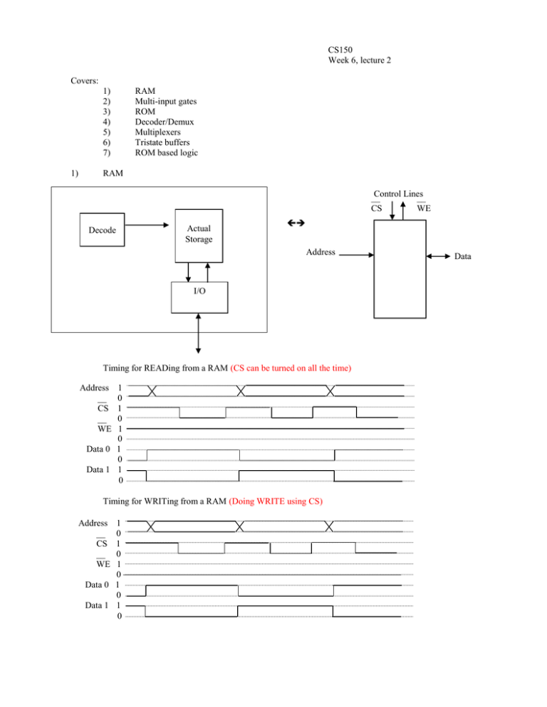
CS150 Week 6, lecture 2 Covers: 1) 2) 3) 4) 5) 6) 7) 1) RAM Multi-input gates ROM Decoder/Demux Multiplexers Tristate buffers ROM based logic RAM Control Lines __ __ CS WE Decode Actual Storage Address I/O Timing for READing from a RAM (CS can be turned on all the time) Address __ CS __ WE 1 0 1 0 1 0 Data 0 1 0 Data 1 1 0 Timing for WRITing from a RAM (Doing WRITE using CS) Address __ CS __ WE 1 0 1 0 1 0 Data 0 1 0 Data 1 1 0 Data SRAM –Static RAM Word lines (from decoder) _ dj dj bit lines 2X3 SRAM SA ? ___ WE 2) ____________________ F(I0, I1, I2, I3, … IN) = (I0 + I1 + I2 + I3 + … + IN) Multi-input gates: Alternative N-input NOR: VCC RBIG I0 I1 I2 I3 I4 I0 VCC I1 GND I6 … I7 IN _____________ G(I0, I1, I2, I3, … IN) = (I0 I1 I2 I3 … IN) Alternative N-input NAND: VCC I5 VCC VCC I2 I3 VCC I4 VCC I5 VCC I6 VCC I7 VCC … IN NOR/NOR/Inverter = AND/OR with inverted inputs: _ A A B Pi 3) ROM 2N Word lines (Internal) N Address Lines Bit lines (M) 8X1 ROM -Hard-wired AND array generates all minterms A B C Decoder Decoder truth table A B C 4) Decoder/Demux n inputs, 1 of 2n outputs. Decoder A0 A1 A2 … A 0 0 0 0 1 1 1 1 B 0 0 1 1 0 0 1 1 C 0 1 0 1 0 1 0 1 A0 A1 A2 A3 A4 A5 A6 A7 1 0 0 0 0 0 0 0 0 1 0 0 0 0 0 0 0 0 1 0 0 0 0 0 0 0 0 1 0 0 0 0 0 0 0 0 1 0 0 0 0 0 0 0 0 1 0 0 0 0 0 0 0 0 1 0 0 0 0 0 0 0 0 1 ABC Decoder truth table IN A 0 0 0 0 1 1 1 1 2n outputs B 0 0 1 1 0 0 1 1 C 0 1 0 1 0 1 0 1 A0 A1 A2 A3 A4 A5 A6 A7 IN 0 0 0 0 0 0 0 0 IN 0 0 0 0 0 0 0 0 IN 0 0 0 0 0 0 0 0 IN 0 0 0 0 0 0 0 0 IN 0 0 0 0 0 0 0 0 IN 0 0 0 0 0 0 0 0 IN 0 0 0 0 0 0 0 0 IN IN is the value of the input, “I” How to make a Demux with a decoder: IN A B A0 A1 Decoder A2 A3 Decoder creates minterms (Maxterms) A B C A 0 0 0 0 1 1 1 1 B 0 0 1 1 0 0 1 1 C 0 1 0 1 0 1 0 1 F1 1 0 0 0 1 0 0 1 F2 0 1 1 1 0 0 0 0 F3 1 1 1 0 1 1 0 1 Decoder F1 (Minterm) F2 (Minterm) F3 (Maxterm) = Remember: 5) 0 1 2 3 4 5 6 7 Multiplexers How to make a multiplexer out of a decoder: S2S1 S0 S1 S0 2n inputs 1 output Decoder I3 I2 I1 I0 6) Tri-state buffers OUT BUFT tri-state truth table T OUT 0 IN 1 Hi-Z (High impedence. Open circuit.) OUT BUF-E tri-state truth table T OUT 0 Hi-Z (High impedence. Open circuit.) 1 IN T IN E IN To select between multiple input lines to put on a single output line: S3 S2 S1 S0 (Only one select line can be on at a time.) IN3 IN2 OUT IN1 IN0 Open collector 7) ROM based logic A 0 0 0 0 1 1 1 1 B 0 0 1 1 0 0 1 1 C 0 1 0 1 0 1 0 1 F1 0 1 1 0 0 1 0 0 F2 0 0 1 1 0 0 0 1 F3 0 1 1 0 1 1 0 0 F4 1 1 1 1 1 1 1 1 K x N ROM implements N different functions of log2K variables. The table above is for a 8x4 ROM. The 3-bit address (A, B, and C) addresses a data record in the ROM. For an address of 000, you’ll get the outputs of functions F 1, F2, F3, and F4 for the input input 000. 64K Serial EEPROMs $3
