®
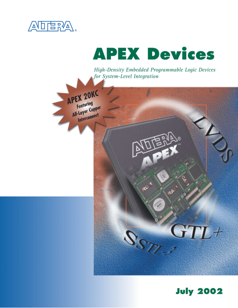
APEX Devices
High-Density Embedded Programmable Logic Devices
for System-Level Integration
0KC
2
X
E
AP eaturing
F
r
Coppe
r
e
y
a
All-L onnect
Interc
July 2002
APEX™ programmable logic devices provide
the flexibility and high density needed for
system-on-a-programmable-chip (SOPC)
applications. Their MultiCore™ architectures
combine the benefits of look-up table (LUT)
logic with embedded memory, saving board
space and simplifying complex system
design. APEX devices also offer True-LVDS™
dedicated circuitry for 840-Mbps data
transfer rates. APEX 20KC devices,
manufactured using all-layer copper
interconnect technology, feature increased
performance to address the high-bandwidth
needs of communications applications.
APEX: A Revolutionary
Embedded Architecture
Figure 2. Improved Performance with APEX 20KC Devices
APEX 20KC
The Altera® APEX device family offers
All-Layer Copper
complete system-level integration on a
MultiCore architecture, APEX FPGAs
combine and enhance the strengths of
APEX 20KE
Performance
single device. With the innovative
Aluminum
APEX 20K
Aluminum
previous programmable logic device (PLD) architectures
FLEX 10KE
Aluminum
and deliver the ultimate in design flexibility and efficiency
for high-performance, SOPC applications (Figure 1). The
new APEX 20KC devices are manufactured on a 0.15 µm
all-layer copper interconnect technology to address the
high-density, high-performance needs of communication
0
0.25-µm
6-layer metal
0.22-µm
6-layer metal
0.18-µm
8-layer metal
0.15-µm
8-layer metal
Process and Metal Layers
applications.
With densities ranging from 30,000 to over 1.5 million
Breakthrough MultiCore Architecture
gates (113,000 to over 2.4 million maximum system
The innovative APEX MultiCore architecture contains two
gates), APEX devices feature performance enhancements
such as copper interconnect technology and multiple
types of PLD structures: the look-up table (LUT) logic of
FLEX® 10K and FLEX 6000 devices and the enhanced
phase-locked loops (PLLs). With the APEX True-LVDS cir-
embedded memory blocks of FLEX 10KE devices. Both
cuitry, this family can achieve data transfer rates up to
structures are combined into a single integrated
840 Mbps and is designed to be 64-bit, 66-MHz PCI and
architecture, eliminating the need for multiple devices,
PCI-X compliant. The 2.5-V APEX 20K devices are fabri-
saving board space, and simplifying the implementation
cated on an advanced 0.22-µm, six-layer-metal SRAM
of complex designs.
process. The 1.8-V APEX 20KE devices, which are a
functional superset of the APEX 20K devices, utilize a
0.18-µm, eight-layer-metal process. The 1.8-V APEX 20KC
devices are fabricated on a 0.15-µm all-layer copper
eight-layer-metal process for improved performance
(Figure 2). Tables 1 to 4 (pages 4 to 5) provide details of
the APEX devices features.
The MultiCore architecture introduces a new level of
hierarchy called the MegaLAB™ structure. Each MegaLAB
structure contains 16 logic array blocks (LABs) that consist
of 10 logic elements (LEs), each of which are used to
implement LUT logic and an advanced embedded
structure called embedded system blocks (ESBs). The
MegaLAB local interconnect ties the 16 LABs and the
ESBs together without using valuable global routing
Figure 1. APEX Device Features
MultiCore Architecture
LUT
Memory
resources. The MegaLAB structures are connected by the
Embedded System Block (ESB)
ESB
Dual-Port RAM
ROM
CAM
FastTrack® interconnect continuous routing structure for
fast, predictable delays.
I/O Features
LVDS SSTL-2/-3
GTL+ HSTL
CTT
LVPECL
AGP
MultiVolt I/O
Clock Management
Up to 4 PLLs
ClockShift Circuitry
ClockBoost Circuitry
ClockLock Circuitry
Altera Corporation
3
Table 1. APEX Device Highlights
Benefit
Feature
840-Mbps data rates
High-speed I/O interface to provide a true system-level programmable solution
All-layer-copper interconnect
Improves performance by 25% to 35% over aluminum-based devices
MultiCore architecture
Integrates LUT logic and memory into a single architecture
Embedded system block (ESB)
Implements dual-port RAM, first-in first-out (FIFO) buffers, ROM, and content-addressible memory CAM
PCI compliance
Meets all specifications for 64-bit, 66-MHz PCI compliance and PCI-X support
Support for emerging I/O standards
Supports LVDS, LVTTL, LVCMOS, GTL+, CTT, AGP, HSTL, LVPECL, and SSTL-2/-3 I/O standards
SignalTap® II logic analysis
Improves verification of chip functionality
Density up to 1.5 million gates
(2.4 million system gates)
Addresses system-level density needs
1.8-V and 2.5-V operation
Reduces power consumption
Up to four phase-locked loops (PLLs)
Supports ClockLock™, ClockBoost™, and ClockShift™ circuitry, 1x to 160x clock multiplication, and
1 to 256 clock division with an extended frequency range
MultiVolt I/O operation
Ideal for mixed-voltage systems
FineLine BGA™ packaging
Area-optimized, better thermal characteristics, high-pin-count BGA offerings, and packaging
migration flexibility
Vertical migration
Addresses changing density without the need to re-spin the board
Table 2. APEX 20KC Device Features (1.8 V)
Device
Maximum system gates
EP20K200C
EP20K400C
EP20K600C
EP20K1000C
1,772,000
526,000
1,052,000
1,537,000
Logic elements (LEs)
8,320
16,640
24,320
38,400
Maximum RAM bits
106,496
212,992
311,296
327,680
2
4
4
4
-7, -8, -9
-7, -8, -9
-7, -8, -9
-7, -8, -9
Phase-locked loops (PLLs)
Speed grades1
Notes:
1
-7 is the fastest speed grade in the APEX 20KC family.
Table 3. APEX 20KE Device Features (1.8 V)
Device
EP20K30E EP20K60E EP20K100E EP20K160E EP20K200E EP20K300E EP20K400E EP20K600E EP20K1000E EP20K1500E
Maximum system gates
113,000
162,000
263,000
404,000
526,000
Logic elements (LEs)
1,200
2,560
4,160
6,400
8,320
11,520
16,640
24,320
38,400
51,840
Maximum RAM bits
24,576
32,768
53,248
81,920
106,496
147,456
212,9924
311,296
327,680
442,368
2
2
2
2
2
4
4
4
4
4
-1, -2, -3
-1, -2, -3
Phase-locked loops (PLLs)
Speed grades1
Maximum user I/O pins
728,000 1,052,000 1,537,000 1,772,000
-1, -2, -3 -1, -2, -3 -1, -2, -3 -1, -2, -3 -1, -2, -3 -1, -2, -3 -1, -2, -3 -1, -2, -3
128
196
246
316
Package
376
408
488
588
708
92
144-Pin FineLine BGA3
208-Pin PQFP4
93
93
93
125
148
151
143
136
151
175
168
92
240-Pin PQFP
324-Pin FineLine BGA
356-Pin BGA
196
92
88
152
246
246
484-Pin FineLine BGA
271
271
316
376
652-Pin BGA
376
408
488
488
488
672-Pin FineLine BGA
376
408
488
508
508
588
708
1,020-Pin FineLine BGA “F33”
4
1
2
3
4
808
Maximum User I/O Pins
144-Pin TQFP2
Notes:
2,392,000
488
808
-1 is the fastest speed grade in the APEX 20K and APEX 20KE families
TQFP: thin quad flat pack
BGA: ball-grid array
PQFP: plastic quad flat pack
Altera Corporation
CAM is commonly used in data communication
Table 4. APEX 20K Device Features (2.5 V)
Device
EP20K100
EP20K200
EP20K400
applications (Table 5). Because the APEX 20KE and
Maximum system gates
263,000
526,000
1,052,000
APEX 20KC CAM functions as a high-speed parallel
Logic elements (LEs)
4,160
8,320
16,640
comparator, it opens up many new applications for
Maximum RAM bits
53,248
106,496
212,992
FPGA designs. APEX CAM supports single match,
1
1
1
-1, -2, -3
-1, -2, -3
-1, -2, -3
252
382
502
Phase-locked loops (PLLs)
Speed grade
Maximum user I/O pins
Package
multiple match, fast multiple match, and ternary CAM.
Each ESB can be configured as a 32-word × 32-bit CAM,
and ESBs can be cascaded to build larger CAMs. The
Maximum User I/O Pins
144-Pin TQFP
101
integrated CAM in APEX 20KE and APEX 20KC devices
144-Pin FineLine BGA
106
offers considerable gains in system performance and
208-Pin PQFP
159
144
240-Pin PQFP
189
174
324-Pin FineLine BGA
252
356-Pin BGA
252
484-Pin FineLine BGA
configuration flexibility relative to discrete CAM solutions.
High-Bandwidth, Low-Voltage I/O
Standards
277
382
The demand for higher system performance and lower
652-Pin BGA
502
672-Pin FineLine BGA
502
supply voltages is growing. APEX 20KE and APEX 20KC
devices support multiple I/O interfacing standards,
including LVTTL, LVCMOS, GTL+, SSTL-3/2, HSTL, AGP,
Table 5. CAM Applications
CTT, LVPECL, and LVDS with performance up to 840 Mbps.
Address translation
Packet header identification
All APEX devices support the Altera MultiVolt™ I/O
Cache tagging
Pattern recognition
interface, which is ideal for mixed-voltage systems.
IP filtering
Switch address mapping
MAC address look-up
VPI/VCI translation in ATM switches
Enhanced Phase-Locked Loops
To increase system-clock rates, APEX 20KE and
Embedded System Block Configuration
Embedded system blocks are the heart of the MultiCore
architecture. The 2,048 programmable bits of each
APEX ESB can be configured as dual-port RAM, ROM,
or content-addressable memory (CAM).
Embedded Dual-Port RAM
APEX ESBs support dual-port RAM with independent
read/write ports, synchronous or asynchronous RAM
operation, and high-speed first-in first-out (FIFO)
performance in a wide range of RAM widths and depths
(128 × 16, 256 × 8, 512 × 4, 1,024 × 2, and 2,048 × 1).
APEX ESBs also support 225-MHz cache RAM performance
APEX 20KC devices feature up to four PLLs with
enhanced ClockLock, ClockBoost, and ClockShift
circuitry. The ClockLock circuitry uses a synchronizing
PLL with an extended frequency range that reduces
clock delay and skew within the device. The ClockBoost
circuitry provides a clock multiplier that allows the
designer to distribute a low-speed clock and to multiply
that clock on the device. It also allows for resourcesharing within the device and enhances device area
efficiency. The ClockShift circuitry provides a
programmable clock delay and phase-shift capability.
High-Bandwidth True-LVDS Support
and ROM performance over 230 MHz. Multiple ESBs can be
The APEX 20KE and APEX 20KC I/O interface meets
combined to build wider and deeper memories.
840-Mbps data transfer rate specifications and has
demonstrated data transfer rates up to 1 gigabits per
High-Performance CAM
seconds (Gbps) under laboratory conditions (Figure 3,
Within APEX 20KE and APEX 20KC devices, ESBs can
page 6). With dedicated built-in True-LVDS circuitry, the
be configured as CAM, a parallel processing memory that
APEX 20KE and APEX 20KC LVDS supports
facilitates fast address search functions. CAM operates like
programmable bandwidths up to 26 Gbps. APEX devices
reverse RAM: while RAM receives an address input and
offer the highest performance, highest bandwidth SOPC
supplies data output, CAM receives data input and supplies
solution for high-speed data transmission designs.
the address that contains the input data.
Altera Corporation
5
Figure 4. Aluminum vs. Copper Delays
Relative Interconnect Delays
Figure 3. APEX 20KE LVDS Running at 1 Gbps Data Transfer Rate*
1.00
0.30
0.15-µm, Aluminum
0.15-µm, Copper
Interconnect Material
conductors. Interconnect delays are 70% lower than
aluminum delays, which translates to significant core
performance improvements as shown in Figure 4.
Copper is also more scalable than aluminum, resulting in
smaller die size, enhanced internal performance, and
*Data taken under laboratory conditions.
Greater Performance with All-LayerCopper Interconnect
speed.
The four APEX 20KC devices range in density from
200,000 to 1 million system gates (526,000 to 1.8 million
maximum system gates) with embedded memory ranging
APEX 20KC devices offer improved internal and I/O
from 106,469 to 327,680 RAM bits. Three new speed
performance to address the high-density, high-
grades (-7, -8, -9) represent the faster performance of
performance needs of communication applications.
these devices.
With internal performance improvements of 25% to 35%
and I/O transmission speeds up to 840 Mbps, these
devices are ideal for applications such as OC-192 and
Intellectual Property & Quartus II
Design Software Simplify Design
SONET SDH protocol, as well as WAN and gigabit
The Quartus® II design software
Ethernet applications.
provides the most comprehensive
APEX 20KC devices build on the state-of-the-art
environment available for SOPC
features offered in the industry-leading APEX 20KE
design. This is because the Quartus II
devices. Combined with the revolutionary MultiCore
software contains a suite of programmable logic design and
architecture, a wide density range, and advanced
verification tools including an integrated embedded
FineLine BGA package offering up to four PLLs and
software development environment and integration to
multiple user-selectable I/Os standards, the APEX 20KC
third-party EDA software. The Quartus II software allows
devices provide even greater system-level integration.
designers to implement advanced device features such as
In the APEX 20KC devices, copper technology replaces
aluminum for routing structure performance enhancements.
CAM, PLL, and LVDS, or to integrate intellectual property
(IP) megafunctions easily.
Copper has low resistivity and better electro-migration
Table 6 shows the highlights of the Quartus II design
characteristics, making it one of the best-known electrical
software version 2.1.
6
Altera Corporation
Table 6. Quartus II Software Version 2.1 Highlights
Benefit
Feature
LogicLock™ Design Methodology Uses block-based design and optimization capabilities to shorten design and verification cycles and
enable team-based design.
PowerFit™ Place-and-Route
Improves productivity by intelligently optimizing designs based on user’s timing specifications and
delivering the fastest compile times in the industry.
Timing Closure Flow
Includes timing closure floorplan editor to display physical timing estimates between nodes in real
time, ability to make powerful path based assignments on critical paths to remove performance
bottlenecks easily, netlist optimization features, and incremental, block-based placement.
SignalProbe™ In-System
Verification
Allows incremental routing of internal nodes to unused or reserved pins for analysis with an external
scope or logic analyzer.
SignalTap® II Embedded
Logic Analyzer
Enables designers to capture internal signal values in-system and running at system speeds without
external probes and without changing user design files.
NativeLink® Integration
Seamless integration of Quartus II software with third-party EDA synthesis and verification software.
SOPC Builder Integration
Integrates SOPC Builder automated system definition and integration tool.
Contact Altera Today
The APEX device family provides a new level of
capability and offers a platform for SOPC applications.
The revolutionary MultiCore architecture brings together
the power of FPGA logic and embedded memory for
system-level integration. Call Altera today to learn more
about this multi-million-gate programmable logic family
or visit the Altera web site at http://www.altera.com.
Altera Corporation
7
®
The Programmable Solutions Company ®
Altera Offices
Altera Corporation
101 Innovation Drive
San Jose, CA 95134
USA
Telephone: (408) 544-7000
http://www.altera.com
Altera European Headquarters
Holmers Farm Way
High Wycombe
Buckinghamshire
HP12 4XF
United Kingdom
Telephone: (44) 1 494 602 000
Altera Japan Ltd.
Shinjuku i-Land Tower 32F
5-1, Nishi-Shinjuku, 6-Chome
Shinjuku-ku, Tokyo 163-1332
Japan
Telephone: (81) 3 3340 9480
http://www.altera.com/japan
Altera International Ltd.
2102 Tower 6
The Gateway, Harbour City
9 Canton Road
Tsimshatsui Kowloon
Hong Kong
Telephone: (852) 2945 7000
Copyright © 2002 Altera Corporation. All rights reserved. Altera, The Programmable Solutions Company, the stylized Altera logo, specific device designations, and all other words and
logos that are identified as trademarks and/or service marks are, unless noted otherwise, the trademarks and service marks of Altera Corporation in the U.S. and other countries. All
other product or service names are the property of their respective holders. Altera products are protected under numerous U.S. and foreign patents and pending applications, mask work
rights, and copyrights.
GB-APEX20K-5.0


