Study on the Effect of Dead Time and its PWM Techniques
advertisement
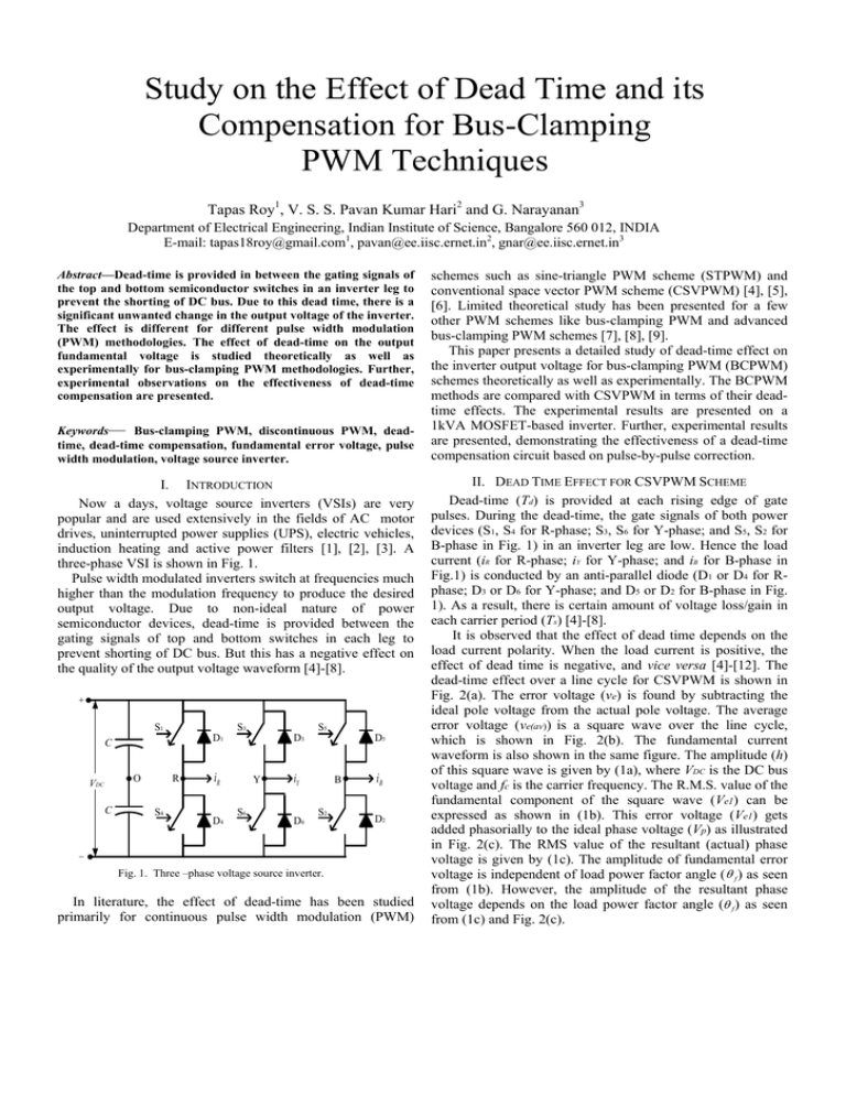
Study on the Effect of Dead Time and its Compensation for Bus-Clamping PWM Techniques Tapas Roy1, V. S. S. Pavan Kumar Hari2 and G. Narayanan3 Department of Electrical Engineering, Indian Institute of Science, Bangalore 560 012, INDIA E-mail: tapas18roy@gmail.com1, pavan@ee.iisc.ernet.in2, gnar@ee.iisc.ernet.in3 Abstract—Dead-time is provided in between the gating signals of the top and bottom semiconductor switches in an inverter leg to prevent the shorting of DC bus. Due to this dead time, there is a significant unwanted change in the output voltage of the inverter. The effect is different for different pulse width modulation (PWM) methodologies. The effect of dead-time on the output fundamental voltage is studied theoretically as well as experimentally for bus-clamping PWM methodologies. Further, experimental observations on the effectiveness of dead-time compensation are presented. Keywords— Bus-clamping PWM, discontinuous PWM, deadtime, dead-time compensation, fundamental error voltage, pulse width modulation, voltage source inverter. I. INTRODUCTION Now a days, voltage source inverters (VSIs) are very popular and are used extensively in the fields of AC motor drives, uninterrupted power supplies (UPS), electric vehicles, induction heating and active power filters [1], [2], [3]. A three-phase VSI is shown in Fig. 1. Pulse width modulated inverters switch at frequencies much higher than the modulation frequency to produce the desired output voltage. Due to non-ideal nature of power semiconductor devices, dead-time is provided between the gating signals of top and bottom switches in each leg to prevent shorting of DC bus. But this has a negative effect on the quality of the output voltage waveform [4]-[8]. + S3 S1 O VDC C S5 D1 C R S4 D3 iR D4 Y S6 D5 iY D6 B S2 iB D2 − Fig. 1. Three –phase voltage source inverter. In literature, the effect of dead-time has been studied primarily for continuous pulse width modulation (PWM) schemes such as sine-triangle PWM scheme (STPWM) and conventional space vector PWM scheme (CSVPWM) [4], [5], [6]. Limited theoretical study has been presented for a few other PWM schemes like bus-clamping PWM and advanced bus-clamping PWM schemes [7], [8], [9]. This paper presents a detailed study of dead-time effect on the inverter output voltage for bus-clamping PWM (BCPWM) schemes theoretically as well as experimentally. The BCPWM methods are compared with CSVPWM in terms of their deadtime effects. The experimental results are presented on a 1kVA MOSFET-based inverter. Further, experimental results are presented, demonstrating the effectiveness of a dead-time compensation circuit based on pulse-by-pulse correction. II. DEAD TIME EFFECT FOR CSVPWM SCHEME Dead-time (Td) is provided at each rising edge of gate pulses. During the dead-time, the gate signals of both power devices (S1, S4 for R-phase; S3, S6 for Y-phase; and S5, S2 for B-phase in Fig. 1) in an inverter leg are low. Hence the load current (iR for R-phase; iY for Y-phase; and iB for B-phase in Fig.1) is conducted by an anti-parallel diode (D1 or D4 for Rphase; D3 or D6 for Y-phase; and D5 or D2 for B-phase in Fig. 1). As a result, there is certain amount of voltage loss/gain in each carrier period (Ts) [4]-[8]. It is observed that the effect of dead time depends on the load current polarity. When the load current is positive, the effect of dead time is negative, and vice versa [4]-[12]. The dead-time effect over a line cycle for CSVPWM is shown in Fig. 2(a). The error voltage (ve) is found by subtracting the ideal pole voltage from the actual pole voltage. The average error voltage (ve(av)) is a square wave over the line cycle, which is shown in Fig. 2(b). The fundamental current waveform is also shown in the same figure. The amplitude (h) of this square wave is given by (1a), where VDC is the DC bus voltage and fc is the carrier frequency. The R.M.S. value of the fundamental component of the square wave (Ve1) can be expressed as shown in (1b). This error voltage (Ve1) gets added phasorially to the ideal phase voltage (Vp) as illustrated in Fig. 2(c). The RMS value of the resultant (actual) phase voltage is given by (1c). The amplitude of fundamental error voltage is independent of load power factor angle (θ f ) as seen from (1b). However, the amplitude of the resultant phase voltage depends on the load power factor angle (θ f ) as seen from (1c) and Fig. 2(c). h = V DC Ve1 = Td = V DC Td f sw TS (1a) 2 2h (1b) π VPDT = V p + Ve1 + 2V p Ve1 cos( 1800 − θ f ) 2 2 (1c) (a) (a) i phase ve(av ) (b) +h Fig. 3. R-phase modulating signals (mR) for (a) 30°BCPWM and (b)60°BCPWM schemes. θ −h 360 ° 180° ve1 (b) Ve1 VPDT 180 0 − θ f θ f = 00 θf Vp Ip A. 30° Bus-clamping PWM scheme (30°BCPWM) In 30°BCPWM scheme, each phase of VSI is clamped to one of the DC bus terminals in the middle 30° duration of each quarter of the fundamental cycle [7], [8], [9]. In the duration of the clamping, there is no switching of power devices in the given leg. Hence dead-time effect is zero during the clamping duration. The average error voltage is also zero in the clamping intervals. In the other intervals, this is equal to +h for negative current, and –h for positive current. Fig. 4(a) illustrates the instantaneous and average error voltages (ve and ve(av)) over a line cycle for power factor 0.866 lagging. As the power factor changes, the waveshape of average error voltage also changes. (c) v phase Fig. 2. (a) Dead-time effect over a line cycle, (b) average error voltage with respect to the fundamental current waveform, (c) phasor diagram illustrating dead-time effect for CSVPWM scheme. DEAD-TIME EFFECT FOR BUS-CLAMPING PWM SCHEMES The modulating signals corresponding to two BCPWM schemes, namely 30° bus-clamping PWM (30°BCPWM) and 60° bus-clamping PWM (60°BCPWM), are presented in Fig. 3(a) and 3(b), respectively. The two methods are studied in terms of their dead-time effects. ve i phase + VDC III. ωt θ f =30° ve(av) TS Td (a) v phase i phase 180°+ θ f 210° 240° Ve1 300° 330° 360°+ θ f V PDT 1650 θ θ f 30° 60° Vp 30 0 Ip 120° 150° ve(av) (c) (b) Fig. 4. (a) Instantaneous error voltage for θ f=30° and (b) average error voltage for 0° ≤ θ f ≤ 30° with 30°BCPWM. The average error voltage for a power factor angle between 0° and 30° (lagging) is illustrated in Fig. 4(b). The amplitude (RMS value) and the phase of the fundamental error voltage for this waveform can be expressed as2h [ 4.535 − 2.928 cos θ f ] π 0.366 sin θ f ] β = 1800 − tan −1[ 1 − 0.366 cosθ f Ve1 = ( 2a) ( 2b) It may be noted that the phase β is measured with respect to the fundamental current. Fig. 5. (a) Magnitude and (b) phase of fundamental error voltage for different ranges of power factor angles (c) Phasor diagram illustrating dead time effect for 30°BCPWM (Ve1=0.6365V, β=165° ) For other ranges of power factor angle Ve1 and β are evaluated in similar fashion. The RMS value (normalized with respect to h) and the phase of the fundamental error voltage vary with power factor (pf) as shown plotted in the Fig. 5(a) and 5(b), respectively. Ve1 remains constant for power factor angles between 30° and 60° as seen from Fig. 5(a). As shown by Fig. 5(b), the phase β varies around 180° , while β is always equal to 180° in case of CSVPWM scheme. The magnitude and phase of the phase voltage get modified due to the dead time effect as seen from the phasor diagram in Fig. 5(c). B. 60° Bus-clamping PWM scheme (60°BCPWM) In case of 60°BCPWM scheme, each phase is clamped to one of the DC bus terminals during the middle 60°duration of each half cycle of its fundamental voltage [7], [8], [9]. Deadtime effect in case of 60°BCPWM can be analysed in a fashion similar to that of 30°BCPWM. The instantaneous and average error voltages are shown in Fig. 6(a). Fig. 6(b) shows the average error voltage for a power factor angle between 0° and 60° lagging. The RMS value and phase of the fundamental error voltage of this waveform are evaluated in the same manner as those for 30°BCPWM. These expressions are given in 3(a) and 3(b) , respectively. h Ve1 = (a) 2h [ 5 − 4 cos θ f ] π β = 1800 − tan −1[ -30° 195° β 180° 165° v phase 60° -90° sin θ f 2 − cosθ f (3a) ] ve i phase + VDC 45° -45° (3b) 90° ωt -60° -50° pf angle (leading) 30° 0° (b) 50° pf angle (lagging) θ f =30° TS Td (a) ve(av) Ve1 v phase i phase 0 180 +θ f 240 0 300 0 V PDT 156 0 360 0+θ f Vp 30 0 θ 60 0 Ip 120 0 ve(av) (b) Fig. 6. (a) Instantaneous error voltage for θ f =30° and (b) average error voltage for 0° ≤ θ f ≤ 60° with 60°BCPWM. The expressions for RMS value and phase of fundamental error voltage (i.e. Ve1 and β ) for other ranges of power factor angle are evaluated in similar way. Fig. 7(a) shows the variation of RMS value (normalized with respect to h) of fundamental error voltage with power factor angle. The RMS error voltage remains constant for power factor angles in between 60° and 90° as seen from this figure. The variation of phase angle β with power factor angle is shown in Fig. 7(b). Similar to 30°BCPWM, the phase β varies around 180° over the whole power factor range. The phasor diagram illustrating the dead-time effect on the fundamental phase voltage for 0.866 lagging power factor is shown in Fig. 7(c). The observations are similar to those in case of 30°BCPWM. Fig. 7. (a) Magnitude and (b) phase of fundamental error voltage for different ranges of power factor angle (c) Phasor diagram of dead time effect for 60°BCPWM (Ve1 =0.5578V, β =156° ). C. Comparison of CSVPWM and BCPWM Fig. 8 shows that the normalized R.M.S. fundamental error voltage is independent of power factor angle for CSVPWM scheme. Fig. 5(a) and 7(a) are reproduced here for comparison with CSVPWM. The three methods are compared at the same carrier frequency. ° θf ° h h h Fig. 8. Comparison of dead- time effect between BCPWM and CSVPWM schemes. From Fig. 8. it can be concluded that the effect of dead-time is lower in case of BCPWM scheme than in case of CSVPWM scheme at a given carrier frequency. Further, for high power factor loads, the 60°BCPWM scheme is better than 30°BCPWM scheme. (a) IV. EXPERIMENTAL RESULTS This section presents experimental results, validating the analysis in the previous section. β pf angle (leading) pf angle (lagging) (b) A. Experimental Set-up A 1kVA MOSFET based three-phase two-level VSI is designed, developed and tested successfully to carry out the experimental validation of dead-time effect. The input to the inverter is a single-phase diode bridge rectifier with an inductive AC-side filter and a capacitive DC-side filter. The DC bus to the inverter acts as output capacitive filter to the rectifier. The PWM pulses are generated by DSP processor TMS320LF2407. The control board takes the PWM signals Time (ms) 5ms/div 1.68A Time (ms) 5ms/div Peak=1.50A 1.50A Time (ms) 5ms/div Load current (A) 1A/div Peak=1.68A Load current (A) 1A/div 1.48A Load current (A) 1A/div Load current (A) 1A/div Peak=1.48A Peak=1.68A 1.68A Time (ms) 5ms/div (a) (b) (c) (d) Fig. 9. Measured load current - (a) without and (b) with dead-time compensation for 30°BCPWM. (c) without and (d) with dead-time compensation for 60°BCPWM. (a) (b) Fig. 10. Harmonic spectra of measured load current - (a) without and (b) with dead-time compensation for 30°BCPWM. and provides the dead-time before feeding to the power board. The load is considered as R-L type. Experimental results are presented without and with deadtime compensation. The compensation circuit for dead-time effect is as presented in [10]. It works on the principle of pulse-by-pulse correction. While this compensation circuit is used for sine-triangle PWM in [10], the same is employed for BCPWM methods here. B. Measured Current Waveforms The load current is measured for an R-L load (R=26.5Ω, L=41mH, resulting in a power factor of 0.9) at a modulation index m=1.0, with VDC=124V, and Td=3.2µs. The carrier frequency fc=30 kHz, and the average switching frequency, fsw=20 kHz. The measured load current waveforms without and with dead-time compensation circuit for 30°BCPWM scheme are shown in Fig. 9(a) and (b), respectively. Since the switching frequency is quite high (20 kHz), the ripple component is negligible in the current waveforms. Further, dead-time compensation improves the distortion around zero-crossing. Also, there is a clear improvement in the peak value of load current. For 60°BCPWM scheme, the experimental conditions are the same as those for 30°BCPWM scheme as mentioned above. Fig. 9(c) and 9(d) show the measured load current waveforms without and with dead time compensation respectively, for 60°BCPWM scheme. The observations are also similar to those for 30°BCPWM scheme. The fundamental current increases with dead-time compensation as seen from Fig. 9(c) and 9(d). Fig. 10(a) and 10(b) present the measured harmonic spectra of load current corresponding to 30°BCPWM scheme without and with dead-time compensation, respectively. These spectra confirm the increase in fundamental current with dead-time compensation. C. Measured Fundamental Current The values of fundamental load current are measured for CSVPWM as well as BCPWM schemes without and with dead-time compensation. The experimental conditions under which the PWM methods are compared are same as those in earlier section except for load and switching frequency. Here the load considered is R=50Ω and L=20mH. The average switching frequencies considered are 3.6, 7, 9, 12, and 15 kHz. The carrier frequency fc is same as the average switching frequency fsw for CSVPWM and is 1.5 times that of fsw for BCPWM methods. The theoretical values of R.M.S. fundamental current for CSVPWM, 30°BCPWM and 60°BCPWM are shown plotted in Fig. 11(a). As seen the fundamental current is reduced on account of dead-time (compared to the ideal values) for all PWM schemes. However, such reduction is lower in case of two bus-clamping PWM methods than CSVPWM. Experimental results, corresponding to the theoretical results in Fig. 11(a), are shown plotted in Fig. 11(b). These measured values agree with the theoretical values. Compared to the theoretical values, the experimental values of RMS fundamental current are found to be lower. This is due to the voltage drops in the switches, which are not considered in the theoretical analysis. However, both theoretical and experimental results show that the fundamental current reduces with increase in switching frequency on account of dead-time. The compensation circuit works reasonably well for all PWM schemes as seen from Fig. 11(c). Again the difference between the ideal load current and compensated load current could be attributed to the voltage drops in the power semiconductor devices. Fundamental load current (A) 0.88 Ideal load current 0.86 60° BCPWM 0.84 0.82 V. CONCLUSIONS This paper analyses the effect of dead-time on the inverter output voltage for bus-clamping PWM schemes. The error voltage amplitude is expressed as a function of dead-time duration, carrier cycle, DC voltage and power factor angle. The analytical study is validated experimentally. The analytical and experimental results show that the effect of dead-time on fundamental voltage is lower in case of busclamping PWM than CSVPWM scheme at high power factors. Dead-time compensation circuit is found to significantly reduce the adverse effect of dead-time on fundamental output voltage for bus-clamping PWM schemes. 30° BCPWM REFERENCES 0.80 CSVPWM 0.78 [1] 0.76 0 5 fsw (kHz) 10 15 [2] (a) 0.90 Ideal load current Fundamental load current (A) 0.88 [3] 0.86 0.84 30° BCPWM 0.82 60° BCPWM [4] 0.80 [5] 0.78 0.76 CSV [6] PWM 0.74 0.72 5 0 15 10 fsw (kHz) [7] (b) 0.90 Fundamental load current (A) [8] Ideal load current 0.88 0.86 CSVPWM 0.84 60° BCPWM 30° BCPWM [9] 0.82 0.80 [10] 0.78 0.76 [11] 0.74 0.72 0 4 6 8 10 fsw (kHz) 12 14 16 (c) Fig. 11. Comparison of CSVPWM and BCPWM schemes (a) theoretical values of fundamental load current (b) experimental values of fundamental load current (c) experimental values of fundamental load current with deadtime compensation. [12] M. Jones, D. Dujic, and E. Levi, “A Four-Motor Drive Supplied from a Triple Three-Phase Voltage Source Inverter,” Proc. Int. Power Electronics and Motion Control Conference, EPE-PEMC2010, pp. 194-200, Sept. 2010. O. Vodyakho and C. C. Mi, “Three-Level Inverter-Based Shunt Active Filter in Three-Phase Three-Wire and Four-Wire Systems,” IEEE Transactions On Power Electronics, Vol. 24, No. 5, pp-1350-1363, May 2009. B. Sarrazin, N. Rouger, J.P. Ferrievx, and J.C. Crebier, “ Cascaded Inverters for Electric Vehicles: Towards a better Management of Traction Chain from the Battery to the Motor?,” Proc. IEEE Int. Sympo., Industrial Electronics (ISIE), pp. 153158, June 2011. S. G. Jeong and M. H. Park, “The Analysis and Compensation of Dead-Time Effects in PWM Inverters,” IEEE Trans. on Industrial Electronics, Vol. 38, No. 2, pp-108-114, April 1991. V. M. Cardenas G., S. M. Horta, R. S. Echararria, “Eliminations of Dead Time Effects in Three-Phase Inverters,” Proc. Inter. Power Electronics Congress, pp-258-262, 1996. L. B. Brahim, “The Analysis and Compensation Dead-Time Effects in Three-Phase PWM Inverters,” IEEE-IECON, 1998, Vol.2. pp-792-797. X. Mao, R. Ayyanar and A. K. Jain, “Dead Time Effect in Two-Level Space Vector PWM Voltage Source Inverters with Large Current Ripple,” IEEE Applied Power Electronics Conference And Exposition (APEC), 2011, pp-679-684. B. A. Welchko, S. E. Schulz, S. Hiti, “ Effects and Compensation of Dead-Time and Minimum Pulse-Width Limitations in Two-Level Voltage Source Inverters,” Proc. Industry Applications Conference 2006, Vol. 2, pp. 889-896. V.S.S.P.K. Hari and G. Narayanan, “Space-Vector-Based Hybrid Pulse Width Modulation Technique to Reduce Line Current Distortion in Induction Motor Drives,” IET Power Electronics, Vol.-5, No-8, pp-1463-1471, Sept. 2012. M. Raghava Krishna And G. Narayanan, “A Dead Time Compensation Circuit For Voltage Source Inverters,” Proc. National Power Electronics Coference (NPEC), Roorkiee 2010. D. Leggate and RJ Kerkman, “ Pulse-based dead time compensator for PWM voltage inverters,”- IEEE Trans. on Industrial Electronic,s Vol. 44, No-2, pp-191-197, April 1997. J. L. Lin, “A New Approach of Dead-Time Compensation for PWM Voltage Inverters,” Proc. IEEE Transactions on Circuits and Systems, Vol. 49, No. 4, pp-476-483, April 2002.

