Document 13513788
advertisement
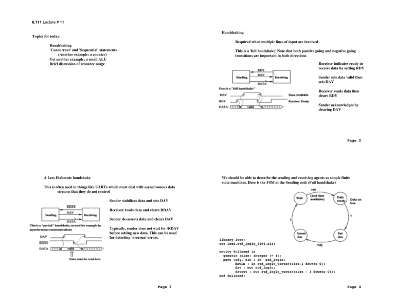
6.111 Lecture # 11 Handshaking Topics for today: Required when multiple lines of input are involved Handshaking 'Concurrent' and 'Sequential' statements (Another example: a counter) Yet another example: a small ALU Brief discussion of resource usage This is a 'full handshake' Note that both positive going and negative going transitions are important in both directions Receiver indicates ready to receive data by setting RDY Sender sets data valid then sets DAV Receiver reads data then clears RDY Sender acknowledges by clearing DAV Page 2 A Less Elaborate handshake We should be able to describe the sending and receiving agents as simple finite state machines. Here is the FSM at the Sending end: (Full handshake) This is often used in things like UARTs which must deal with asynchronous data streams that they do not control Sender stabilizes data and sets DAV Receiver reads data and clears RDAV Sender de-asserts data and clears DAV Typically, sender does not wait for /RDAV before setting new data. This can be used for detecting 'overrun' errors. library ieee; use ieee.std_logic_1164.all; entity fullsend is generic (size: integer := 4); port (rdy, clk : in std_logic; datin : in std_logic_vector(size-1 downto 0); dav : out std_logic; datout : out std_logic_vector(size - 1 downto 0)); end fullsend; Page 3 Page 4 architecture behavioral of fullsend is type StateType is (wt, dat, d_av, r_dy); attribute enum_encoding of StateType: type is "00 01 11 10"; signal state : StateType; begin dav <= '1' when (state = d_av) or (state = r_dy) else '0'; handshake : process(clk) begin if rising_edge(clk) then case state is when wt => if rdy = '1' then state <= dat; else state <= wt; end if; when dat => datout <= datin; state <= d_av; when d_av => state <= r_dy; when r_dy => if rdy = '0' then state <= wt; else state <= r_dy; end if; end case; end if; end process handshake; end; And here is the FSM for the receiving end: library ieee; use ieee.std_logic_1164.all; entity fullrecv is generic (size: integer := 4); port (dav, rclk : in std_logic; datin : in std_logic_vector(size-1 downto 0); rdy : out std_logic; datout : out std_logic_vector(size - 1 downto 0)); end fullrecv; Page 5 architecture behavioral of fullrecv is type StateType is (w_dav, datav, r_rdy, wt_ndav); attribute enum_encoding of StateType: type is "00 01 11 10"; signal state : StateType; begin rdy <= '1' when (state = w_dav) or (state = datav) else '0'; handshake : process(rclk) begin if rising_edge(rclk) then case state is when w_dav => if dav = '1' then state <= datav; else state <= w_dav; end if; when datav => datout <= datin; state <= r_rdy; when r_rdy => state <= wt_ndav; when wt_ndav => if dav = '0' then state <= w_dav; else state <= wt_ndav; end if; end case; end if; end process handshake; end; Page 6 Here is an alternative way of writing an emulator for the '163 counter This is a register which can hold 4 bits Counts when P=T=1, holds when P*T=0 Loads data when /LD = 0 Clears data when /CL = 0 All of these are synchronous: occur only on clock edges (positive edges) Daisy-chaining is possible: RCO connects to T of next most signifigant ctr RCO is T * Q3 * Q2 * Q1 * Q0 Here is an entity statement for this part -- '163 emulator library ieee; use ieee.std_logic_1164.all; use work.std_arith.all; entity ctr is generic (size: integer := 4); port (n_clr, n_ld, p, t, clk : in std_logic; data: in std_logic_vector(size-1 downto 0); count: out std_logic_vector(size-1 downto 0); rco : out std_logic); end ctr; Page 7 Page 8 architecture behavioral of ctr is signal cnt_int : std_logic_vector(size - 1 downto 0); signal int_cnt : std_logic_vector(size - 1 downto 0); signal all_ones : std_logic_vector(size downto 0); begin -- behavioral all_ones <= (others => '1'); rco <= '1' when (t & cnt_int) = all_ones else '0'; count <= cnt_int; DESIGN EQUATIONS (11:32:34) -- internal count rco = t * count_2.Q * count_1.Q * count_0.Q * count_3.Q logical:process(p, t, n_clr, n_ld, cnt_int, data) begin if n_clr = '0' then Note two processes here: int_cnt <= (others => '0'); elsif n_ld = '0' then int_cnt <= data; One has the combinatorics elsif p = '0' or t = '0' then associated with the logic in the part. int_cnt <= cnt_int; else The other has the state transition int_cnt <= cnt_int + 1; dynamics associated with the clock end if; edge. end process logical; state_transition:process(clk) begin if rising_edge(clk) then cnt_int <= int_cnt; end if; end process state_transition; end behavioral; count_3.D = t * count_2.Q * count_1.Q * count_0.Q * n_clr * n_ld * p * /count_3.Q + n_clr * n_ld * /p * count_3.Q + /count_0.Q * n_clr * n_ld * count_3.Q + /count_1.Q * n_clr * n_ld * count_3.Q + /count_2.Q * n_clr * n_ld * count_3.Q + /t * n_clr * n_ld * count_3.Q + n_clr * /n_ld * data_3 count_3.C = clk count_2.D = t * /count_2.Q * count_1.Q * count_0.Q * n_clr * n_ld * p + count_2.Q * n_clr * n_ld * /p + count_2.Q * /count_0.Q * n_clr * n_ld + count_2.Q * /count_1.Q * n_clr * n_ld + /t * count_2.Q * n_clr * n_ld + n_clr * /n_ld * data_2 Page 9 Page 10 RESOURCE ALLOCATION count_2.C = clk (11:32:34) Information: Macrocell Utilization. count_1.D = t * /count_1.Q * count_0.Q * n_clr * n_ld * p + count_1.Q * n_clr * n_ld * /p + count_1.Q * /count_0.Q * n_clr * n_ld + /t * count_1.Q * n_clr * n_ld + n_clr * /n_ld * data_1 Description Used Max ______________________________________ | Dedicated Inputs | 8 | 8 | | Clock/Inputs | 1 | 1 | | Enable/Inputs | 0 | 1 | | Output Macrocells | 5 | 8 | ______________________________________ 14 / 18 = 77 count_1.C = clk count_0.D = t * /count_0.Q * n_ clr * n_ld * p + count_0.Q * n_clr * n_ld * /p + /t * count_0.Q * n_clr * n_ld + n_clr * /n_ld * data_0 count_0.C = clk This was implemented on a 16V8 Here are some numbers relating to how much of the resources of that part we used. % Information: Output Logic Product Term Utilization. These are just about what you would have expected. Note a lot of fluff has been optimized away. Page 11 Node# Output Signal Name Used Max ________________________________________ | 12 | count_3 | 7 | 8 | | 13 | count_2 | 6 | 8 | | 14 | count_1 | 5 | 8 | | 15 | count_0 | 4 | 8 | | 16 | rco | 1 | 8 | | 17 | Unused | 0 | 8 | | 18 | Unused | 0 | 8 | | 19 | Unused | 0 | 8 | ________________________________________ 23 / 64 = 35 % Page 12 Simulation of Tri-State as an Output library ieee; use ieee.std_logic_1164.all; use work.std_arith.all; -- needed for integer + signal entity test_tri is port(clk, oe, cnt_enb : in std_logic; counter : buffer std_logic_vector(3 downto 0); data : inout std_logic_vector(3 downto 0)); end test_tri; architecture foo of test_tri is -- signal counter : std_logic_vector(3 downto 0); begin process (oe, counter) begin if (oe = '1') then data <= counter; else data <= "ZZZZ"; -- N.B. Z must be UPPERCASE! end if; end process; process (clk) begin if rising_edge(clk) then if (oe = '0') and (cnt_enb = '1') then counter <= counter + 1; end if; end if; end process; end architecture foo; Note that data(3 downto 0) are white (meaning an input) when oe is low. Page 13 Now we are going to consider a strictly combinatoric circuit: an Arithmetic Logic Unit (ALU) It takes 2 numbers (quite narrow in this case: 2 bits each) (Plut a carry-in bit) And can add, subtract and shift left This can be done in more than one way. Consider addition: 1. a_int <= '0' & a b_int <= '0' & b if c_in = 0, c <= a_int + b_int if c_in = 1, c <= a_int + b_int + 1 2.. a_int <= '0' & a & c_in b_int <= '0' & b & c_in c_int <= a_int + b_int c <= c_int(width downto 1) These have differences in the way they are implemented, and when we get to actual implementation of the full alu we will find yet another one library ieee; use ieee.std_logic_1164.all; use work.std_arith.all; -- needed for integer + signal entity alu is port(cin : in std_logic; a, b : in std_logic_vector(1 downto 0); alu_ctl : in std_logic_vector(1 downto 0); c : out std_logic_vector(2 downto 0)); end alu; Page 15 Page 14 Here is one architecture for the adder architecture justright of alu is signal a_int, b_int : std_logic_vector(2 downto 0); constant add : std_logic_vector(1 downto 0) := "00"; constant sub : std_logic_vector(1 downto 0) := "01"; constant shift: std_logic_vector(1 downto 0) := "10"; begin a_int <= '0' & a; Note the carry bit is b_int <= '0' & b; used to determine small_alu: process(a_int, b_int, cin, alu_ctl) which expression to begin evaluate: in logic it is a case alu_ctl is kind of multiplexor. when add => if cin = '0' The 'opcode' is another then c <= a_int + b_int; multiplexor: in this else c <= a_int + b_int + 1; end if; case a 3:1 when sub => c <= a_int - b_int; These have overhead. when shift => if cin = '0' then c <= a_ int + a_int; else c <= a_ int + a_int + 1; end if; when others => c <= (others => '-'); end case; end process small_alu; end architecture justright; Page 16 architecture justright of alu is Here is the second architecture: does the same thing... architecture justright of alu is signal a_int, b_int, c_int : std_logic_vector(3 constant add : std_logic_vector(1 downto 0) := constant sub : std_logic_vector(1 downto 0) := constant shift: std_logic_vector(1 downto 0) := begin a_int <= '0' & a & cin; b_int <= '0' & b & cin; small_alu: process(a_int, b_int, cin, alu_ctl) begin case alu_ctl is when add => c_int <= a_int + b_int; when sub => c_int <= a_int - b_int; when shift =>c_int <= a_int + a_int; when others => c_int <= (others => '-'); end case; end process small_alu; c <= c_int(3 downto 1); end architecture justright; downto 0); "00"; "01"; "10"; This may or may not have more overhead. Note that by adding Cin to both inputs (the first place after the binary point is of value ) we save at least some notational overhead. It cancels on subtract. But we have to discard the rightmost bit at the end signal a_int, b_int, c_int : std_logic_vector(3 downto 0); signal a_1, n_b, upper, lower : std_logic_vector(3 downto 0); constant add : std_logic_vector(1 downto 0) := "00"; constant sub : std_logic_vector(1 downto 0) := "01"; constant shift: std_logic_vector(1 downto 0) := "10"; begin a_int <= '0' & a & cin; b_int <= '0' & b & cin; Here our final operation is just an a_1 <= '0' & a & '1'; n_b <= '1' & (not b) & '1'; addition, so we do more work in upper: process(a_int, a_1, alu_ctl) the earlier stages, such as doing begin the two's complement for the case alu_ctl is when add => upper <= a_int; negative of b. We use the same when sub => upper <= a_1; trick for concatenating the carry when shift => upper <= a_int; in bit to both halves of the when others => upper <= (others => '-'); end case; addition. end process upper; lower: process(a_int, b_int, n_b, alu_ctl) begin case alu_ctl is when add => lower <= b_int; when sub => lower <= n_b; when shift => lower <= a_int; when others => lower <= (others => '-'); end case; end process lower; c_int <= upper + lower; c <= c_int(3 downto 1); end architecture justright; Page 17 Page 18 Here is the second of the two schemes Here is a schematic of the way the first of these schemes is implemented. The final selection is a 9:3 MUX, while there are two 6:3 MUXes ahead of it. And ahead of that are some simple combinatoric circuits to generate the sums. Page 19 There still is a MUX: this time of 12:4, but it still has only two 'steering' bits. We discard a bit in the final result And we also have to construct the signals that come to this MUX from the left. Page 20 Here is the first of the three schemes Information: Macrocell Utilization. This is the third option: here we have two 12:4 MUXes and only a simple addition to reconstruct things. Some logic is required to put together the signals at the left. Description Used Max ______________________________________ | Dedicated Inputs | 1 | 1 | | Clock/Inputs | 4 | 4 | | I/O Macrocells | 7 | 64 | | Buried Macrocells | 3 | 64 | | PIM Input Connects | 12 | 312 | ______________________________________ 27 / 445 = 6 % We discard a bit at the output CLOCK/LATCH ENABLE signals Input REG/LATCH signals Input PIN signals Input PINs using I/O cells Output PIN signals Total PIN signals Macrocells Used Unique Product Terms Required 0 0 5 2 5 12 8 43 Max (Available) 4 69 5 2 62 69 128 640 Page 21 This is the second of the three schemes This is the third of the three schemes Information: Macrocell Utilization. Information: Macrocell Utilization. Description Used Max ______________________________________ | Dedicated Inputs | 1 | 1 | | Clock/Inputs | 4 | 4 | | I/O Macrocells | 6 | 64 | | Buried Macrocells | 2 | 64 | | PIM Input Connects | 12 | 312 | ______________________________________ 25 / 445 = 5 CLOCK/LATCH ENABLE signals Input REG/LATCH signals Input PIN signals Input PINs using I/O cells Output PIN signals Total PIN signals Macrocells Used Unique Product Terms Page 22 Required 0 0 5 2 4 11 6 28 Description Used Max ______________________________________ | Dedicated Inputs | 1 | 1 | | Clock/Inputs | 4 | 4 | | I/O Macrocells | 5 | 64 | | Buried Macrocells | 1 | 64 | | PIM Input Connects | 8 | 312 | ______________________________________ 19 / 445 = 4 % Max (Available) 4 69 5 2 62 69 128 640 CLOCK/LATCH ENABLE signals Input REG/LATCH signals Input PIN signals Input PINs using I/O cells Output PIN signals Total PIN signals Macrocells Used Unique Product Terms Page 23 Required 0 0 5 2 3 10 4 28 % Max (Available) 4 69 5 2 62 69 128 640 Page 24

