Design for Test of Digital Systems Course Outline
advertisement
Course Outline
Introduction; Manufacturing, Wafer sort, Final test, Board and System
Test, Defects, and Faults
Design for Test of Digital Systems
TDDC33
Test generation; combinational and sequential test generation
Design-for-Test techniques; test point insertion, scan, enhanced scan
Test data compression, Built-In Self-Test; Logic BIST and memory
BIST
System Chip Test; test architectures, test planning, test scheduling,
and power constraints
Erik Larsson
System Test and Boundary Scan
Department of Computer Science
Problems
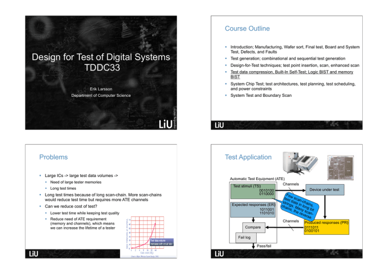
Test Application
Large ICs -> large test data volumes ->
Automatic Test Equipment (ATE)
Channels
Test stimuli (TS)
Device under test
0010100
0110000
Few
tes sca
stri t data n-chai
Expected responses (ER)
cha ngs. M in longns,
ins, any
b
1011001
the
s it
rev can1101010
ers
e.
Channels Produced responses (PR)
Compare
0111011
0100101
Need of large tester memories
Long test times
Long test times because of long scan-chain. More scan-chains
would reduce test time but requires more ATE channels
Can we reduce cost of test?
Lower test time while keeping test quality
Reduce need of ATE requirement
(memory and channels), which means
we can increase the lifetime of a tester
Fail log
Pass/fail
3
May 8, 2008
52
Interface ATE-DUT: probes that
contact die are sensitive. Test data
must be transported correctly;
other wise, a good IC can be classified
as defective.
ATE-based testing
Advantages with ATE-based testing
Alternatives
Test data compression
High quality test
Built-In Self-Test
Diagnosis possible
Logic BIST and Memory BIST
Disadvantages with ATE-based testing
ATEs are expensive
Important aspects:
Interface between ATE and device-under-test
Test stimuli
Low throughput due to:
Test responses
Long scan-chains
Low test shift speed
Limited number of channels
Limited tester memory
Many systems need
testing frequently. Some
at power-on.
Only possible to test at manufacturing
6
Test generation
D-Algorithm
G3
Example: Create test for output connected to Vdd
Fault-free
0
X
0
W
NOR
U
NOR
G5
G
AND
X
Stuck-at 0
Faulty
OR
Z
F
G4
Y
H
AND
Initialize the circuit by placing X on each line
Vdd
X
0
A
B
G1
G2
1
For a SA0, X=D and A=B=0 (for the selected fault)
Propagate D through G2
Select a sensitizing path (we select G3)
To propagate through G3, we let U=0
Don’t care bit
Propagate through G5
Reached a primary output with D
Justify values on H, Y, U, W. H=0 (ok). F=0? Conflict! Select Y=0
Analysis of Scan Test
Analysis of Scan Test
ATPG first creates test cubes
Then, convert cubes to vectors by filling don’t cares
Fault simulate vectors to mark off additional faults
Merged for several faults; many unspecified don’t care values
0
scan chain
0 1
Logic
Under Test
scan chain
1
1
0
= don’t care
0
scan chain
1
0 1
Logic
Under Test
fault 1
1 0
scan chain
0
fault 2
scan chain
0
1
0
1
1 0
0
scan chain
1
= fill values
= care
1
fault 1
0
fault 2
fault 3
0
fault 3
0
1
= care
9
10
Care-Bit Example
Test data compression
For all modules
Care-bit density varies from test to test
Example: 15,624 scan cells, 1,764 tests
Very many patterns
with few care bits
(many don’t care bits)
Source: O. Farnsworth et al., IBM
11
Fill test stimuli don’t care bits
Simulate to find test responses
Compress test stimuli
Design decompression logic
Design compactor
vector {stimuli} {expected response}
vector {stimuli} {expected response}
1
{1xx xx0 xxx} {x0x xxx x11}
1
{111 110 000} {x0x xxx x11}
2
{xx1 xx1 xxx} {1xx 0xx xxx}
2
{001 111 111} {1xx 0xx xxx}
3
{0x0 xxx xxx} {xxx 1xx xxx}
3
{000 000 000} {xxx 1xx xxx}
Test data compression
Test data compression
For all modules
For all modules
Fill test stimuli don’t care bits
Fill test stimuli don’t care bits
Simulate to find test responses
Simulate to find test responses
Compress test stimuli
Compress test stimuli
Design decompression logic
Design decompression logic
Design compactor
Design compactor
vector {stimuli} {expected response}
vector {stimuli} {expected response}
vector {stimuli} {expected response}
{compressed stimuli}
1
{111 110 000} {x0x xxx x11}
1
{111 110 000} {101 100 011}
1
{111 110 000} {101 100 011}
{001 010 101}
2
{001 111 111} {1xx 0xx xxx}
2
{001 111 111} {100 010 010}
2
{001 111 111} {100 010 010}
3
{000 000 000} {xxx 1xx xxx}
3
{000 000 000} {010 101 100}
3
{000 000 000} {010 101 100}
Test data compression
Test data compression
For all modules
Fill test stimuli don’t care bits
Simulate to find test responses
Compress test stimuli
Design decompression logic
Design compactor
SoC
Module under test
ATE (test stimuli)
0 0 1 0 1 0 1 0 1
vector {stimuli} {expected response}
{compressed stimuli}
1
{111 110 000} {101 100 011}
{001 010 101}
2
{001 111 111} {100 010 010}
3
{000 000 000} {010 101 100}
-
-
-
-
-
-
-
-
-
-
-
-
-
-
-
-
-
-
1
Decompression
Few ATE channels and
many (short) scan-chains
lead to shorter test times
1
0
0
MISR
-
-
-
-
-
-
-
-
-
-
-
-
Test data compression
Test Compression Categories
MISR (produced)
Test Stimulus Compression
1
Code-based schemes
0
0
Linear decompression
Broadcast scan
11
Test Response Compaction
00
MISR (expected)
10
Space compaction
Faulty module!
1
0
Time compaction
Space/time compaction
Handling of Xs
1
Code-based Schemes
Fixed-to-Fixed
The original test stimuli are partitioned into n-bit blocks to form symbols. These
symbols are encoded using variable-length code words. Statistical coding
such as Huffman code.
Variable-to-Fixed
The original test stimuli are partitioned into n-bit blocks to form symbols. The
symbols are then encoded with code words. Each code word have b bits. (b<n
to get compression). Dictionary codes.
n
Fixed-to-Variable
Dictionary Code (Fixed-to-Fixed)
The original test stimuli are partitioned into variable length symbols, and the
codewords are each b-bits long. Ex. Run-Length Code
Variable-to-Variable
The test stimuli are partitioned into variable length symbols, and the symbols
are partitioned into variable length code words. Ex. Golomb Code.
Scan chain 0
Tester
b
Dictionary
Scan chain 1
Scan chain 2
Scan chain n
Driving Multiple Scan Chains
Dictionary Generation
TD = { t1, t2, …, tn }
Goal: include as many words as possible in the dictionary
l : length of a scan chain (bits)
Limit the size of the dictionary
m : number of scan chains
Selective entries
Data word : m-bit long
ATE
Find compatible words and properly map the Xs in the test set
m
l
Compatibility
1 1 0 1 0 0
0 1 1 1 0 0
Decoder
M
I
S
R
0 1 0 1 0 0
1 1 1 0 0 1
If any pair of words in a set are compatible, this set can be mapped
to a single word
0
X
0
X
X
1
X
X
0
X
0
0
0
1
0
0
Dictionary Generation
Test Response Analysis: Test Data
Compression and BIST
Problem: find |D| disjoint subsets containing pair-wise
compatible words, such that the total number of the words in
these subsets is maximized
How store/analyze test responses on-chip?
Clique partitioning problem
Heuristic solution
vertex
Compaction – does loose information
Compaction alternatives:
NP-complete
1
3
11
4
Parity check
7
clique
12
Compression – does not loose information
15
One counting
Transition counting
Signature analysis
8
2
5
16
14
9
6
13
edge
10
Maximal
clique
Parity check
One counting
Pi-1
Test
Patterns
CUT
ri
11110000
11001100
AND
OR
11101010
(5)
OR
11111111
(8)
10101010
+
D
Q
SA1
Q
Clk
11110000
11001100
AND
10101010
Parity check is simple but lossy (in respect to information).
Example of ”one counting”. The result from the fault free circuit
is ”5” and the result from a faulty circuit is 8.
Transition counting
Signature analysis
ri
Test
Patterns
CUT
D
Q
ri-1
+
Counter
Q
Clk
Count the number of transitions and compare at the end of the
testing with the correct number of transitions for a fault-free
circuit.
Signature analysis is the most commonly used test response
compaction technique. It was proposed by N. Benowitz et al.,
”An advanced fault isolation system for digital logic”, IEEE
Transactions on Computers, Vol. C-24, No. 5, pp. 489-497.
Serial-input signature register (SISR) and parallel signature
analysis using multiple-input signature register (MISR).
Parallel signature analysis
FF
FF
+
M
FF
+
Example, L=4, XOR-network gives
SISR:
+
A single-input signature register (SISR) takes one input and
compacts it to an L-bit sequence.
+
Serial signature analysis
FF
FF
FF
f(x)=1+x+x4.
General form: f(x)=a0x0+a1x1+a2x2+a3x03+a4x4. And with
a0=a1=a04=1 and a2=a3=0, f(x)=1+x+x4
+
FF
+
r0
FF
FF
FF
r1
r2
r3
M0
M1
+
M
FF
M2
+
MISR:
FF
M3
Compaction Options
Response Compaction: Motivation
MISR (Multiple-Input Signature Register)
Compaction of test responses necessary for
verifying the test response
Very high compression ratio
Store compacted response called signature and
compare to known fault-free signature
BUT: does not tolerate x-states in test responses
May require product logic re-design OR
X-state gating logic
Fault-free
signature
(W bits)
Error information loss can impact diagnostics
Combinational space compaction
N >> W
XOR-network
Can be x-state tolerant (e.g., X-Compact from Intel)
Test
response
(N bits)
Less compression
Possibly better for diagnostics
31
Response
compaction
circuit
=
Pass/fail
Space Compaction
X-compact
Compress test response in the spatial dimension
Compress k-bit-wide response stream to q-bit signature stream
(k >> q)
Space compactor is a combinational circuit
Space
compactor
.
.
.
s1
s2
k >> q
sq
Time Compaction
Serial signature analysis
Compress test responses in the temporal dimension
Compress m-bit (or word) test response stream to q-bit (or
word) signature stream
Time compactor is a sequential circuit (finite-state machine)
b1b2…bm
Time
compactor
M
+
zk
.
.
.
FF
+
z1
z2
r0
Assume: f(x)=1+x+x4, Start
pattern (seed): {0000}, Faultfree test response sequence
M={10011011}, gives R={1011}
Faulty test response:
M’={10001011} gives R’={1110},
and M’’={10011011} gives
R’’={1011}
s1s2…sq
The faulty response M’ results
in R’ which is different from R
while the response R’’ from M’’
is not different from R.
The fault detection problem (M
and M’’) is called aliasing.
FF
FF
FF
r1
r2
r3
Start pattern
M r 0 r 1 r2 r 3
M’ r0 r1 r2 r3
M’’ r0 r1 r2 r3
1 0
1 1
0 1
1 0
1 1
0 0
0 1
1 0
R1
1 0
1 1
0 1
1 0
0 1
0 0
1 1
1 1
R’ 1
1 0
0 1
1 0
1 1
0 1
0 1
1 0
1 0
R1
0
0
1
1
0
0
1
1
0
0
0
0
1
1
0
0
1
1
0
0
0
0
1
1
0
0
1
0
0
1
1
0
0
1
1
1
0
0
0
1
1
0
0
1
1
0
0
0
0
1
1
0
0
0
Final signature
0
0
1
0
1
0
1
1
0
0
0
0
1
0
1
0
1
1
0
0
0
0
1
0
1
0
1
Aliasing Problem
Unknows (X)
Loss of fault information is inevitable in response compaction
Output from analog blocks
Aliasing occurs when fault-free response and faulty response
map to the same signature, i.e. fault is not detected (masked)
by the compaction process
Memories and non-scan storage elements
Aliasing reduces fault coverage (even when complete test sets
are used) and makes fault coverage hard to determine
Combinational feed-back loops
Asynchronous set/reset
Tristate buses
False paths (not normal functional paths)
Critical paths
Multi-cycle paths
Floating ports
Bidirectional I/O
X-handling
MISR Gate
X-Blocking; block X’s at source (where it is generated)
from
scan chain
Requires masking data
msk=‘0’ blocks x-states
X source
Compactor
AND
msk
msk=‘1’ propagates test
responses
Trade-offs required
select
One mask value for all chains
(simple)
X-Masking; block X’s in front of compactor
Scan chain 0
AND
Mask
controller
Compactor
Vector with unique mask value
for each chain (complex)
to
MISR
40
X-State Gating
Alternatives
Data in
Controls
Test data compression
Built-In Self-Test
Stimulus de-compression logic
Scan chain
Scan chain
Scan chain
Logic BIST and Memory BIST
Important aspects:
Test stimuli
Test responses
Mask/select logic
Response compaction logic
Data out
41
Built-In Self-Test
42
On-chip/off-chip
ATE
Key component to discuss:
Test pattern storage/generation
Test stimuli storage/generation
Off-chip
Test source
Device under test (DUT)
Test sink
Test response analysis
Test control
In a non-BIST environment:
test generation is performed by ATPG; a tool such as FastScan can
generate deterministic test patterns,
test stimuli and expected test responses are stored in the ATE, and
the ATE controls the testing and performs test evaluation.
Test source
On-chip
Test sink
Device under test (DUT)
DUT1
Test Application
Test source
DUT1
Device under test
(DUT)
Test Application
Test source
Test controller
Test sink
Test sink
DUT2
DUT2
ATE
Test source
Device under test
(DUT)
Device under test
(DUT)
Test source
Test controller
Test sink
Device under test
(DUT)
Test sink
DUTn
Let ATE start tests and
analyze final results
Test source
DUTn
Device under test
(DUT)
Test source
Test controller
Test sink
Device under test
(DUT)
Test sink
Test Pattern Generation
Test Pattern Generation
How store/generate test patterns on-chip?
Exhaustive test generation; simple hardware (a counter), 100%
fault coverage but too time consuming
Deterministic test patterns
Deterministic test generation; high fault coverage but requires
ATE for test pattern storage
Exhaustive test patterns
Pseudo-exhaustive/random test patterns
Pseudo-exhaustive test generation using Linear-Feedback
Shift-Registers (LFSR)
Random test patterns
Commercial tools usually make use of a random test generation
for 60-80% of the faults (easy to detect) and deterministic test
generation for the remaining part (hard to detect)
+
FF
FF
FF
FF
Test Pattern Generation
Random Pattern Resistant Faults
+
FF
FF
FF
FF
FF
+
FF
0001
1000
0100
1010
0101
0010
0001
1000
0100
1010
0101
0010
0001
1000
0100
1010
FF
The effectiveness of a test is given based on the test’s fault
coverage, length, and hardware/data storage requirement.
FF
Probability to create a 1 at the output; 1/2n where n is the
number of inputs. n=2; P=0.25, n=4; P=0.0625
0001
1100
0110
0011
1101
1010
0101
1110
0111
1111
1011
1001
1000
0100
0010
0001
AND
AND
50
Random pattern resistance
STUMPS: Self-testing using MISR and
parallel shift register sequence generator
Some logic takes too long to test with pseudo-random patterns
Too many specific input bit values are required
LFSR
Too many pseudo-random trials needed to achieve the required
value combination
51
Scan chain 3
Scan chain 2
Scan chain 1
Scan chain 0
MISR
Test source: Linear Feedback
Shift Register (LFSR)
Test sink: Multiple Input
Signature Register (MISR)
Test-per-clock/scan (cycle)
+
FF
+
+
+
+
Change registers so they become
test sources and test sinks. Some
registers can act as test source and
test sink (but not at the same time).
Test-per-clock
Register
Test controller determines when a
register should be test source or
test sink.
Logic
Register
Register
Logic
Logic
The test controller determines the
test schedule; when each logic
block should be tested.
Optimization problem to find lowest
test time without violating
constraints.
Register
Register
Test time
Logic
FF
Response compaction:
FF
FF
FF
FF
FF
FF
FF
+
FF
0001
1000
0100
1010
0101
0010
0001
1000
0100
1010
0101
0010
0001
Scan chain 3
FF
FF
Scan chain 2
Scan chain 1
Scan chain 0
FF
FF
+
FF
+
Test generation:
+
FF
SC3
+
+
+
Built-In Self-Test (BIST)
Make register test generator/compactor -> test-per-clock
Test-per-clock
Change registers so they become test sources and test sinks.
Some registers can act as test source and test sink (but not at
the same time).
Test controller determines when a register should be test
source or test sink.
The test controller determines the test schedule; when each
logic block should be tested.
Optimization problem to find lowest test time without violating
constraints.
Test time
Register
56
Alternatives
Testing Memories
Memory testing is an increasingly important issue
Test data compression
RAMs are key components for electronic systems
Built-In Self-Test
Memories represent about 30% of the semiconductor market
Logic BIST and Memory BIST
Embedded memories are dominating the chip yield
Memory testing is increasingly difficult
Important aspects:
Growing density, capacity, and speed
Test stimuli
Emerging new architectures and technologies
Test responses
Embedded memories: access, diagnostics & repair, heterogeneity,
custom design, power & noise, scheduling, compression, etc.
Cost drives the need for more efficient test methodologies and
automation
Failure analysis, fault simulation, ATPG, diagnostics BIST/BIRA
(Built-In Redundancy Analyzer)/BISR (built-in self repair)
57
Testing Memories
Fault Models for Memory Test
Data Inputs
Write drivers
Problems
Classical fault models are not sufficient to represent all important
failure modes in RAM
Decoders
Address Inputs
Sequential ATPG is not possible for RAM
Scan is too expensive
Memory array
But,
Memories are, different to logic, composed of regular structures
(memory cells)
Functional fault models are commonly used for memories
Sense Amplifiers
Data Outputs
Fault Models for Memories
Fault Models for Memories
Stuck-At Fault (SAF)
Bridging Fault (BF)
Cell (line) SA0 or SA1
A stuck-at fault (SAF) occurs when the value of a cell or line is
always 0 (a stuck-at-0 fault) or always 1 (a stuck-at-1 fault)
A test that detects all SAFs guarantees that from each cell, a 0 and
a 1 must be read.
Transition Fault (TF)
Cell fails to transit from 0 to 1 or 1 to 0 in specified time period
A cell has a transition fault (TF) if it fails to transit from 0 to 1 or
from 1 to 0.
Fault Models for Memories
A bridging fault (BF) occurs when there is a short between two cells
AND-type BF
OR-type BF
Stuck-Open Fault (SOF)
A stuck-open fault (SOF) occurs when the cell cannot be accessed
due to, e.g., a broken word line
A read to this cell will produce the previously read value
Coupling Fault (CF)
A coupling fault (CF) between two cells occurs when the logic value
of a cell is influenced by the content of, or operation on, another cell
State Diagram Representation
w0
Address-Decoder Fault (AF)
An address decoder fault (AF) is a functional fault in the address
decoder that results in one of four kinds of abnormal behavior:
Given a certain address, no cell will be accessed
A certain cell is never accessed by any address
Given a certain address, multiple cells are accessed
A certain cell can be accessed by multiple addresses
w1
0
w0,w1
1
w1
w0,w1
0
1
SA0
SA1
w0
Fault-free memory cell
w0
w0, w1
0
1
w1
w1
0
1
w0
Rising TF
Falling TF
w1, w0
Memory Test
March Test Notation
A memory test is a finite sequence of test elements
: address sequence is in the ascending order
: address changes in the descending order
: address sequence is either or
A test element contains a number of memory operations (access
commands)
Data pattern (background) specified for the Read and Write operation
Address (sequence) specified for the Read and Write operations
A march test algorithm is a finite sequence of march elements
A march element is specified by an address order and a finite
number of Read/Write operations
r: the Read operation
Reading an expected 0 from a cell (r0); reading an expected 1 from
a cell (r1)
w: the Write operation
Writing a 0 into a cell (w0); writing a 1 into a cell (w1)
Example (MATS+): { (w0); (r0,w1); (r1,w0)}
Zero-One Algorithm (MSCAN)
Galloping Pattern (GALPAT)
Zero-One Algorithm [Breuer & Friedman 1976]
Complexity is 4N**2
Also known as MSCAN
All AFs,TFs, CFs, and SAFs are located
For SAF
Solid background (pattern)
1. Write background 0;
Complexity is 4N
2. For BC = 0 to N-1
{ Complement BC;
For OC = 0 to N-1, OC != BC;
{ Read BC; Read OC; }
Complement BC; }
3. Write background 1;
4. Repeat Step 2;
Classic Test Algorithms
Classic Test Algorithms
MSCAN, complexity 4N: { (w0); (r0); (w1);
Checkerboard Algorithm, complexity 4N
(r1)}
Zero-one and checkerboard algorithms do not have sufficient
coverage
Galloping Pattern (GALPAT), complexity 4N2
Other algorithms are too time-consuming for large RAM
Sliding (Galloping) Row/Column/Diagonal (Based on GALPAT,
but instead of a bit, a complete row, column, or diagonal is
shifted), complexity 4N1.5
Test time is the key factor of test cost
Butterfly Algorithm, complexity 5NlogN
March test algorithms
Complexity ranges from N2 to NlogN
Need linear-time test algorithms with small constants
Moving Inversion (MOVI) Algorithm, for functional and AC
parametric test, Functional (13N) and Parametric (12NlogN)
Surround Disturb Algorithm
N=number of bits
Test Time
March Test
Zero-One (MSCAN) [Breuer & Friedman 1976]
{ (w0); (r0); (w1); (r1)}
Memory size
Complexity of test algorithm
Size
N
10N
NlogN N1.5
N2
1M
0.01s
0.1s
0.2s
11s
3h
Modified Algorithmic Test Sequence (MATS) [Nair, Thatte & Abraham
1979], { (w0); (r0, w1); (r1)}
16M
0.16s
1.6s
3.9s
11m
33d
MATS+ [Abadir & Reghbati 1983], { (w0);
64M
1.5h
1.43y
(r0, w1);
(r1, w0)}
0.66s
6.6s
17s
256M 2.62s
26s
1.23m 12h
23y
Marching 1/0 [Breuer & Friedman 1976]
{ (w0); (r0, w1, r1); (r1, w0, r0); (w1); (r1, w0, r0); (r0, w1, r1)}
1G
10.5s
1.8m
5.3m
366y
MATS++ [Goor 1991], { (w0);
4G
42s
7m
22.4m 32d
57c
March X, { (w0);
915c
March C [Marinescu 1982],
{ (w0); (r0, w1); (r1, w0); (r0);
16G
2.8m
28m
1.6h
4d
255d
(r0, w1);
March C- [Goor 1991],
{ (w0); (r0, w1); (r1, w0);
(r0, w1);
(r1, w0, r0)}
(r1, w0); (r0)}
(r0,w1); (r1, w0) (r0)}
(r0,w1); (r1, w0) (r0)}
Memory BIST
Memory BIST (MBIST)
Memories are one of the most universal cores
Methodology
In Alpha 21264, cache RAMs represent 2/3 transistors and 1/3
area; in StrongArm SA110, the embedded RAMs occupy 90% area
[Bhavsar, ITC-99]
Processor-based BIST
In average SOC, memory cores represent more than 90% of the
chip area by 2010 [ITRS 2000]
Programmable
Hardwired BIST
Embedded memory testing is increasingly difficult
High bandwidth (speed and I/O data width)
Fast
Compact
Interface
Heterogeneity and plurality
Serial (scan, 1149.1)
Isolation (accessibility)
Parallel (embedded controller; hierarchical)
AC test, diagnostics, and repair (The primary difference between
DC stuck-at scan and AC scan is the clocking during the sample
cycle. For AC scan, only the launch and capture of a signal need to
be at-speed. In DC scan, all are slow)
Patterns (address sequence)
March
Pseudorandom
BIST is considered the best solution
MBIST Architecture
Summary
Test data compression
Explore high number of don’t care bits to compress test data
Add decompressor logic to system
BIST
Analyze response in system
MUX
Built-In Self-Test (BIST)
Store/generate test vectors in system
LOGIC
MEMORY
TEST COLLAR
Analyze response in system
Logic BIST and Memory BIST
MUX
Testing can be performed in-field
0
75
76
