Document 13135881
advertisement
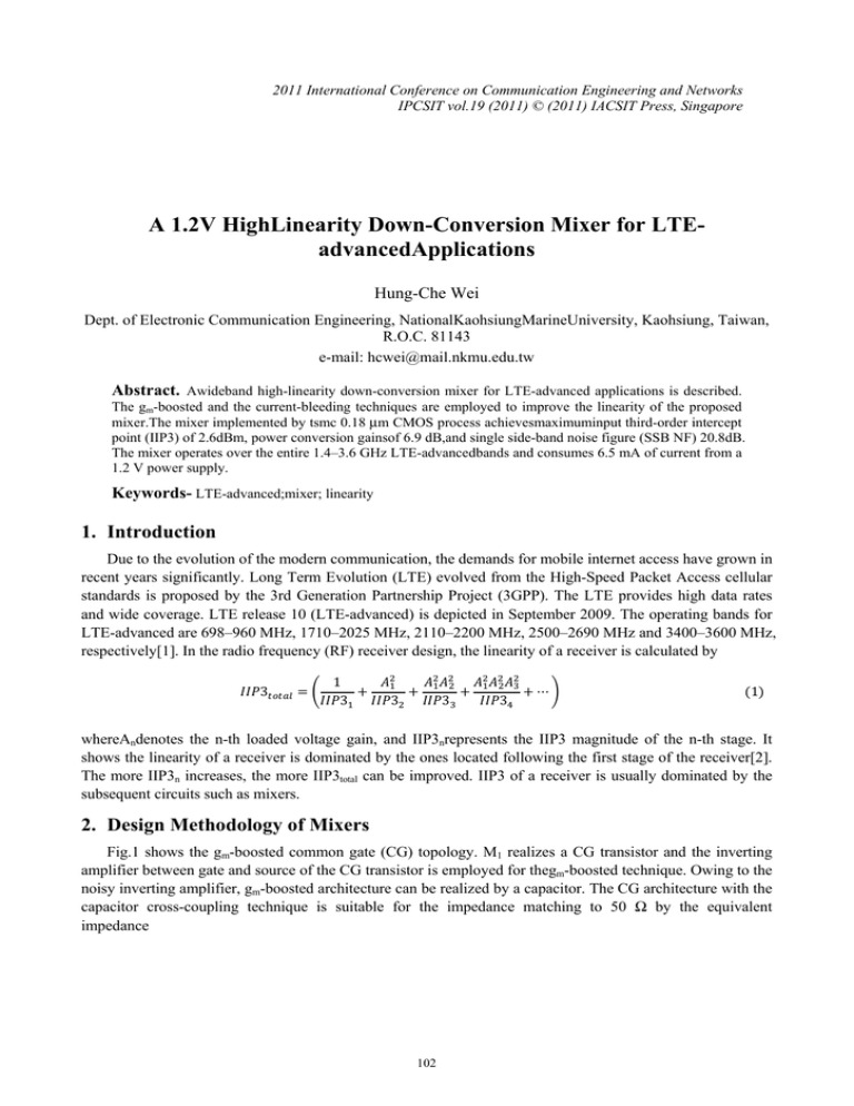
2011 International Conference on Communication Engineering and Networks IPCSIT vol.19 (2011) © (2011) IACSIT Press, Singapore A 1.2V HighLinearity Down-Conversion Mixer for LTEadvancedApplications Hung-Che Wei Dept. of Electronic Communication Engineering, NationalKaohsiungMarineUniversity, Kaohsiung, Taiwan, R.O.C. 81143 e-mail: hcwei@mail.nkmu.edu.tw Abstract. Awideband high-linearity down-conversion mixer for LTE-advanced applications is described. The gm-boosted and the current-bleeding techniques are employed to improve the linearity of the proposed mixer.The mixer implemented by tsmc 0.18 μm CMOS process achievesmaximuminput third-order intercept point (IIP3) of 2.6dBm, power conversion gainsof 6.9 dB,and single side-band noise figure (SSB NF) 20.8dB. The mixer operates over the entire 1.4–3.6 GHz LTE-advancedbands and consumes 6.5 mA of current from a 1.2 V power supply. Keywords- LTE-advanced;mixer; linearity 1. Introduction Due to the evolution of the modern communication, the demands for mobile internet access have grown in recent years significantly. Long Term Evolution (LTE) evolved from the High-Speed Packet Access cellular standards is proposed by the 3rd Generation Partnership Project (3GPP). The LTE provides high data rates and wide coverage. LTE release 10 (LTE-advanced) is depicted in September 2009. The operating bands for LTE-advanced are 698–960 MHz, 1710–2025 MHz, 2110–2200 MHz, 2500–2690 MHz and 3400–3600 MHz, respectively[1]. In the radio frequency (RF) receiver design, the linearity of a receiver is calculated by 3 1 3 3 3 3 1 whereAndenotes the n-th loaded voltage gain, and IIP3nrepresents the IIP3 magnitude of the n-th stage. It shows the linearity of a receiver is dominated by the ones located following the first stage of the receiver[2]. The more IIP3n increases, the more IIP3total can be improved. IIP3 of a receiver is usually dominated by the subsequent circuits such as mixers. 2. Design Methodology of Mixers Fig.1 shows the gm-boosted common gate (CG) topology. M1 realizes a CG transistor and the inverting amplifier between gate and source of the CG transistor is employed for thegm-boosted technique. Owing to the noisy inverting amplifier, gm-boosted architecture can be realized by a capacitor. The CG architecture with the capacitor cross-coupling technique is suitable for the impedance matching to 50 Ω by the equivalent impedance 102 Fig. 1.gm m-boosted CG topology. 1 1 2 Due to the gm-boostted CG and the t capacitorr cross-couplling techniquue, the CG aand common source (CS)) c be realizedin a gm-bboostedcapaccitor cross-ccouplingtranssconductor sttage and thee third-orderr topologies can intermodulaation (IM3)oof a transconnductor staggecan be sup ppressed[3,4]]. However, the overall gain of thee topology is attenuated by b the CG toppology. The gain and lin nearity of thee gm-boosted CG can be improved i byy adopting thee current-bleeding techniqque[5]. The prooposed high-linearity mixxer with a gm-boosted currrent-bleedinng transconduuctor stage iss depicted inn Fig. 2. Thee gm-boosted current-bleeedingtransconnductor stag ge consists of o M1–M4, C1–C4, L1–L2 and R1–R2. M1–M4and operatein thhesaturationrregion. C1 and a C2 are the cross-coouplingcapaccitors.M3 and d M4are thee current-bleeeding transisttors and imprrove the convversion gain and IIP3 of the proposedd mixer. R1 and a R2are thee wideband innputmatchingg network of RFport. Duue to the feeedback matcchingnetworkk of the RF port, p the RF F port does not n require thhe external biasvoltage.T b Thegm-boosteed current-blleedingtranscconductor staage convertss the input RF R voltage siignals into sm mall output current sign nals to the coommutating stage. The commutating c g stage is ofteen driven by the power froom local osccillator(LO) in i the RF front-end. The ccommutating gstage whichh consists of M5–M8acts as ideal sw witches whenn the input LOpower L is large. If thhe LOpower issmall, thee commutatinngstageacts as an amplifieer. The DC operation poin nt and the asppect ratio of Fig. 3..Proposed mixxer with the gm m-boosted currrent-bleedinggtranscoductorr stage. the com mmutatingstagge will influeence the requuirement of thedriven t LO O power. Thee transistors are a biased inn the boundarry between the t saturationn region andd the triode reegion to makke M5–M8 acct as ideal sw witches withh lower drivenn power. The RF signal is injected frrom the sourrce of M5–M8, then the IF F current signal is down-103 converted by the commutating stage with the multiplied function. is translated into the voltage signal by The load stage consisted of M9, M10, R3 and R4translates the down-converted current signal into the voltage signal. R1 and R2 can provide output impedance and M9 and M10can provide appropriate voltage swing headroom.The proposed gm-boosted current-bleeding transconductor stage compensatesthe IM3 phenomenon by adjusting the bleeding current and cross-coupling capacitors. However, the bleeding current also increases the power consumption of the mixer. In the mixer design, the trade-offs between IIP3, conversion gain and NFare the main design considerations.Due to the NF of the receiver is dominated by the NF of the low noise amplifier, the proposed mixer can be optimized inthe aspects of linearity and conversion gain. 3. Simulation Results The simulator for the circuit simulation is Agilent Advance Design System (ADS) 2009. The proposed mixer is realized by tsmc 0.18 μm Mixed Signal CMOS RF model. The RF is from 1.4 GHz to 3.6 GHz in the simulation of the proposed mixer, Due to the fixed IF of 10 MHz, the LO frequency is from 1.39 GHz to 3.59 GHz. The active current of the mixer is about 6.5 mA from a 1.2 V supply voltage. In order to the mixer performance,the three terminals of RF, LO and IF ports are matching to 50-Ω. As shown in Fig. 4, the maximum conversion gain reached the peak value of 8.3 dB at the RF of 2.3 GHz when the LO power is –5 dBm. To optimize the overall performance of the proposed mixer, the LO power is –8 dBm . The conversion gain of the proposed mixer is 4.3–6.9 dB and the SSB NF is 20.8–23.2 dB. IIP3 of the mixer is calculated by using a two-tone testing. The frequencyspacing in the two-tone test is set to be 300 kHz which is thechannel spacing in a LTE-advanced system. Fig. 5 illustrates CG and IIP3versus RF. The conversion gainsare 4.3–6.9dB.Theextrapolation plot of IIP3 is illustrated in Fig. 6 andthe maximum measured IIP3 Fig. 4.Conversion gain versus LO power at different frequencies. Fig. 5.Conversion gain (CG) and IIP3 versus RF. 104 Fig. 6.IIP3 characteristic at 3.6 GHz. achieves 2.6dBm at 3.6 GHz andthe minimum IIP3 is –0.6 dBm at 1.4GHz.The simulation results of other mixers are compared by thesame design consideration in optimizing the linearity. Table Isummarizes the simulation results of the proposed mixer. Theproposed mixer reveals excellent properties oflinearity and power consumption. TABLE I. PERFORMANCE SUMMARY OF MIXERS. Ref. This work [6] [7] 0.18 0.18 0.18 Supply Voltage (V) 1.8 1.8 1.2 fRF(GHz) 1.9 2.4 1.4–3.6 fLO(GHz) 1.95 2.25 1.39–3.59 Currentconsumption (mA) 23.56 14.5 6.5 LO Power (dBm) –1.2 4 –8 IIP3 (dBm) 20.45 8.6 –0.5–2.6 P-1dB (dBm) 12.8 1 –12.9––13.9 Conversion Gain (dB) 1.65 -5.3 4.3–6.9 SSB Noise Figure (dB) 17.2 17.5 20.8–23.2 Process (μm) 4. Conclusion A 1.2 V high-linearityCMOS mixer with the gm-boosted current-bleedingtranscondutor stage is presented. The proposedmixer operates at the RF of 1.4–3.6 GHz, the LO frequency of1.39–3.59 GHz, and IF of 10 MHz, respectively. The mixer is realizedby adopting the linearity compensation method based on the gm-boosted current-bleedingtransconductor. Both of the conversion gain and the linearity are improved. The mixerconsumes 7.8mW from a 1.2 V power supply. The simulation results of the proposed mixer exhibitsmaximum power conversion gain of 6.9 dB, IIP3 of 2.6dBm, and singleside-band noise figure of 20.8dB. The proposed mixer revealshigh conversion gain and IIP3 and is suitable forLTE-advanced applications. 5. Acknowledgment This work was supported by National Science Council, Taiwan, underthe Grant NSC99-2218-E-022-002. The chip fabricationwas supported by the National Chip Implementation Center of Taiwan,R.O.C. 6. References 105 [1] M.J. Chang, Z. Abichar and C.-Y. Hsu, “WiMAX or LTE: Who will Lead the Broadband Mobile Internet?,” IT Professional, vol. 12, no. 3, pp. 26–32, 2010. [2] W. H. Hayward, Introduction to Radio Frequency Design, Upper Saddle River, NJ: Prentice-Hall, 1982. [3] J. Jeong, J. Kim, D. S. Ha and H.-S. Lee, “A reliable ultra low power merged LNA and Mixer design for medical implant communication services,” IEEE Life Science Systems and Applications Workshop (LiSSA), pp. 51–54, Apr. 2011. [4] Z. Lei, M. Kim and Y. Yang, “A common-gate down-conversion mixer with capacitive cross-coulping technique for UHF RFID applications,” IEEE Microwave Technology & Computational Electromagnetics (ICMTCE), pp. 277–280, May 2011. [5] S. G. Lee and J. K. Choi, “Current-reuse bleeding mixer,” IEE Electronics Letters, vol. 36, no. 8, pp. 696–697, Apr. 2000. [6] N. Islam, S. K. Islam and H. F. Huq, “High performance CMOS converter design in TSMC 0.18-μm process,” IEEE Proceedings of Southeast Conference, pp. 148–152, Apr. 2005. [7] S.-Y. Chao and C.-Y. Yang, “A 2.4-GHz 0.18-μm CMOS doubly balanced mixer with high linearity,” IEEE International Symposium onVLSI Design, Automation and Test, pp. 247–250, Apr. 2008. 106

