Document 12915634
advertisement
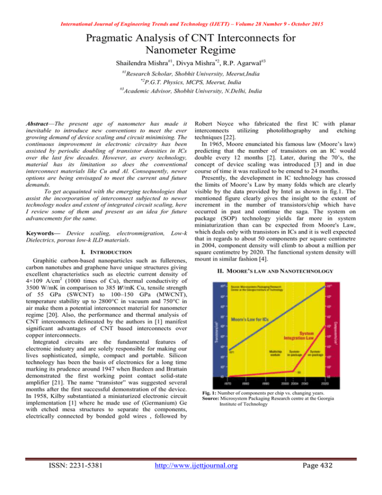
International Journal of Engineering Trends and Technology (IJETT) – Volume 28 Number 9 - October 2015 Pragmatic Analysis of CNT Interconnects for Nanometer Regime Shailendra Mishra#1, Divya Mishra*2, R.P. Agarwal#3 #1 Research Scholar, Shobhit University, Meerut,India *2 P.G.T. Physics, MCPS, Meerut, India #3 Academic Advisor, Shobhit University, N.Delhi, India Abstract—The present age of nanometer has made it inevitable to introduce new conventions to meet the ever growing demand of device scaling and circuit minimising. The continuous improvement in electronic circuitry has been assisted by periodic doubling of transistor densities in ICs over the last few decades. However, as every technology, material has its limitation so does the conventional interconnect materials like Cu and Al. Consequently, newer options are being envisaged to meet the current and future demands. To get acquainted with the emerging technologies that assist the incorporation of interconnect subjected to newer technology nodes and extent of integrated circuit scaling, here I review some of them and present as an idea for future advancements for the same. Keywords— Device scaling, electronmigration, Low-k Dielectrics, porous low-k ILD materials. I. INTRODUCTION Graphitic carbon-based nanoparticles such as fullerenes, carbon nanotubes and graphene have unique structures giving excellent characteristics such as electric current density of 4×10⁹ A/cm2 (1000 times of Cu), thermal conductivity of 3500 W/mK in comparison to 385 /mK Cu, tensile strength of 55 GPa (SWCNT) to 100–150 GPa (MWCNT), temperature stability up to 2800°C in vacuum and 750°C in air make them a potential interconnect material for nanometer regime [20]. Also, the performance and thermal analysis of CNT interconnects delineated by the authors in [1] manifest significant advantages of CNT based interconnects over copper interconnects. Integrated circuits are the fundamental features of electronic industry and are solely responsible for making our lives sophisticated, simple, compact and portable. Silicon technology has been the basis of electronics for a long time marking its prudence around 1947 when Bardeen and Brattain demonstrated the first working point contact solid-state amplifier [21]. The name ―transistor‖ was suggested several months after the first successful demonstration of the device. In 1958, Kilby substantiated a miniaturized electronic circuit implementation [1] where he made use of (Germanium) Ge with etched mesa structures to separate the components, electrically connected by bonded gold wires , followed by ISSN: 2231-5381 Robert Noyce who fabricated the first IC with planar interconnects utilizing photolithography and etching techniques [22]. In 1965, Moore enunciated his famous law (Moore’s law) predicting that the number of transistors on an IC would double every 12 months [2]. Later, during the 70’s, the concept of device scaling was introduced [3] and in due course of time it was realized to be emend to 24 months. Presently, the development in IC technology has crossed the limits of Moore’s Law by many folds which are clearly visible by the data provided by Intel as shown in fig.1. The mentioned figure clearly gives the insight to the extent of increment in the number of transistors/chip which have occurred in past and continue the saga. The system on package (SOP) technology yields far more in system miniaturization than can be expected from Moore's Law, which deals only with transistors in ICs and it is well expected that in regards to about 50 components per square centimetre in 2004, component density will climb to about a million per square centimetre by 2020. The functional system density will mount in similar fashion [4]. II. MOORE’S LAW AND NANOTECHNOLOGY Fig. 1: Number of components per chip vs. changing years. Source: Microsystem Packaging Research centre at the Georgia Institute of Technology http://www.ijettjournal.org Page 432 International Journal of Engineering Trends and Technology (IJETT) – Volume 28 Number 9 - October 2015 The graph illustrated in fig. 2 shows the number of transistors in typical Intel chips over the years (42 million in the Pentium 4 chip) which is in accordance with the straight line Moore’s Law prediction. However, an increment in the number of transistors per chip is to accompany the reduced transistor size. Consequently, the manufacturing process must Fig. 2: Minimum feature size vs. changing years. Source: http://barrett- group.mcgill.ca /tutorials/nanotechnology/ nano03.htm It is further estimated that by 2040, wire linewidths will be on the order of carbon nanotubes, and by 2060, features will be the size of individual atoms which will be no more in coalition with Moore’s Law [6]. The reason behind this flaw is not the physical barriers which cause Moore's prediction to collapse, but rather economic ones as an immense amount of economic burden levied is due to the stringent clean-room conditions required and the cost of fabrication increases geometrically, as does computer power. This completely must not be misled to the conclusion that the computer industry will catastrophically collapse in the near future, but rather signifies that our current way of doing things needs a notion. The industry needs to adapt to new technologies in order to create future generation computers such as new micro- and nanofabrication techniques, to build conventional transistors ever smaller. An entirely new fabrication techniques, which, for instance, circumnavigate current cleanroom requirements, or exploit clever computer processing paradigms, carving out a niche for more research in Nanotechnology. coupling capacitance between adjacent wires, which was ignored in past is now significant. The frequency-dependent resistance and inductance (i.e., the skin effect) of each conductor can be readily obtained by subdividing the cross section of each conductor into many segments, replacing each segment by a resistor and inductor in series, and then reducing the aggregate resistors and inductors through a circuit formulation [9]. Apparently, as we move towards UDSM regime it is realised that increase in chip density is not feasible without fast and dense interconnects. The conventional interconnect materials such as Cu/Al wires cannot be fast or dense simultaneously as a smaller cross-section increases electrical resistance, while greater height or width increase parasitic capacitance with neighbouring wires resulting RC delay [10] . Besides, at higher frequencies they are also subjected to flaws such as electronmigration, electron scattering against rough edges of metallic wires, which is ineluctable with atomic-scale wires [11]. IV. SEMICONDUCTOR DEVICE: SCALING LIMITS The device scaling is obtained attaining high package density, speed, chip functionality and power improvements. This assists to obtain reduced component dimensions resulting the incorporation of increased number of transistors on to the chip as mentioned by Gordon Moore in the 1975 IDEM (International Electron Device Meeting held in 1972). However, an Intel researcher realize in 1995 that on-chip interconnect scaling is the bottleneck to high-performance integrated circuits [12]. The ongoing process of technical III. INTERCONNECTS: A LIMITING FACTOR In past, on-chip interconnect wires were not considered to be a major issue and had only been considered in special cases or when performing high-precision analysis [7]. However, with the introduction of deep-submicron semiconductor technologies, there have been rapid changes. While the gate delay used to dominate the net delay, the on-chip interconnects delay now account for up to 60% of the total delay in a deep submicron design [8]. The on-chip interconnect delay needs to be accurately quantified; as any error in the on-chip interconnect delay can translate into a large portion of error in the total delay. Another phenomenon that occurs in a deep submicron design is that in order to maintain proper resistance (and therefore voltage drop) in each conducting wire, the conductor’s height is not reduced, if at all, as fast as the width. Due to the different aspect ratio, the ISSN: 2231-5381 Fig.3: Number and lengths of chips bought per dollar Forecast Source: Lenly Group advances is interspersed with claims of delay, power and other improvements in semiconductor design and interconnect potentials. As of 2015 10nm devices are still under commercial development [13]. There are a wide range of technologies being evaluated for the sub-10nm node such as: http://www.ijettjournal.org Page 433 International Journal of Engineering Trends and Technology (IJETT) – Volume 28 Number 9 - October 2015 1. Gate-all-around FETs (also called nanowires) 2. Quantum well FETs 3. Silicon-on-insulator FinFETs 4. Gate-all-around FETs However there are certain technical flaws to be overcome before these can venture the sub 10nm node: 1. As we approach the 7nm node Ge boast of a promising channel option but assumes certain difficulties of adapting germanium for the n channel despite of its excellent response as p channel material. 2. Semiconductors of III-V group which were supposed to be divulged at 10nm, are now being extended to 7nm or 5nm owing to manufacturing difficulties. 3. EUV is still a major constraint as a result of power problem. 4. Gate-all-around claims for improving transistor performance but suffers from reliability and dimension challenges. 5. Graphene or carbon nanotubes still needs to be explored as material for complex CMOS logic devices. 6. SRAM cells scale at a rate of 10% smaller per node shrink. 7. Constituents of ICs such as I/O and contact pads don’t really scale at all. Beside technical aspect economic factor also limits the developmental process as ―node‖ merely quantifies for a group of technologies that deliver an improvement rather than a measure of half-pitch or gate length [14]. These practical limits can be easily visualized by the illustration in fig.3 which is based on the report by The Lenly Group in 2014 depicting the optimal balance of cost and power for 2015 devices with respect to 28nm node. The report suggests that mid-range devices are highly cost sensitive and 28nm node provides the maximum number of transistors per dollar [14]. V. DEVICE SCALING AND INTERCONNECTS The device scaling is obtained attaining high package density, speed, chip functionality and power improvements. The requirement of interconnect technology is to continue meeting the performance requirements for ICs fabricated for succeeding technology generations and varies with the intended function of the interconnect net and the technology used to fabricate the wires. As requirements increase, it necessitates for interconnect considered as part of a system including package and the silicon chip to satisfy the total technology need for the IC. Technological advancements accompanies the increment in RC delay, a crucial parameters for high performance products. The scaled wires in the local and intermediate wiring levels exhibit moderate increase in RC, however fixed length interconnects of semiglobal and global wiring are much more sensitive and need the introduction of repeaters to keep the RC delay within viable limits. However, the effective measure comes with a trade-off with additional chip area and increment in power consumption. ISSN: 2231-5381 An alternate approach may introduce modifications such as modular architectures to reduce the need for fixed length lines such as the dual- or multi-core architecture in state-of-the-art microprocessors. Here, parallel data processing in the multicores allows comparable or even higher processor performance at lower core frequencies and reduced power consumption as compared to a single core high performance processor. However, such significant modifications to circuit architecture comes with an added requirement of needing new design tools and new software and are not generally applicable to all designs. While RC delay is a major factor for many digital applications, capacitive coupling in the local and intermediate levels is an exceedingly cautious issue for low power applications. Crosstalk and noise associated with reducing geometrical facets and increasing currents are becoming a larger problem for both digital and analog circuits. These trends are the bottlenecks of design strategy, and should be considered in that context. In addition to the problems with scaled wires for clock and signaling, an equally difficult problem for interconnect is circuit power distribution. Increasing supply current, related to the decreasing Vdd, causes a substantial increment in voltage drop between the power supply and the bias point for fixed length wires. This problem cannot be solved as easily as the repeater solution for the fixed length clock and signal wires [15]. VI. INTERCONNECT ADAPTATIONS TO MEET TECHNOLOGY REQUIREMENTS From the previous section it is fair and justified that an appropriate interconnect technology should be realized to meet the new device integration requirement. To facilitate the inclusion of extremely small devices, interconnects need to be limited to 10 nm in diameter. However, as the diameters of metallic interconnect wires are scaled down to the limits of the mean free path of electrons flaws like surface scattering from the boundaries of ultra-narrow conductors and the grain boundary scattering may obstruct electronic conduction in the wires [16] thereby affecting the performance improvement as desired from scaling. In addition, electromigration resulting from movement of lots of electrons and electron scattering also mounts. In-order to facilitate the concept of scaling and introduction of newer devices various potential interconnect technologies amidst nanowires, carbon nanotubes and quantum wire are being extensively researched to attain low resistivity, large current carrying capacity, easy of fabrication, and sequestration with low-k dielectric materials for ultra-high density applications [17]. An intentional effort to overcome materials’ restrictions in on-chip electrical interconnects is realized by introducing additional levels of metal such as 13 for 14nm node intel microprocessors and 15 layers for 22nm node power chips by IBM. Besides, complex ―airgap‖ structures are also incorporated in dielectric stack [18]. Low-k Dielectrics such as Carbon Doped Oxide (CDO or SiOC or SiOC:H) with k~3.0 are integrated into interconnect stacks which can be further http://www.ijettjournal.org Page 434 International Journal of Engineering Trends and Technology (IJETT) – Volume 28 Number 9 - October 2015 improvised by using SiOC in conjugation with air in a stack resulting in an integrated k value weighted by the percent of the volume taken up by each phase which all together results in significant amount of reduction in capacitance delays [18]. Hence it is aimed to find materials exhibiting lower resistivity for metal lines, porous low-k ILD materials and advance processes to assimilate these into existing technology [19]. VII. CONCLUSION In due course of study it is realized that certain new conventions, materials and strategies need to be followed by the interconnect technology if we continue the feature of device scaling and minimizing circuitry in order to get accustomed to newer technology nodes. ACKNOWLEDGMENT This research paper has been solely made possible by the unconditional support of my family and few intellectuals who have really bestowed me with their presence in my life like Dr. R.P. Agarwal, Dr. B.K. Kaushik, Mr. Dinesh Chandra Mr. Manoj Kumar Majumder and Mr. Ramesh. Their overwhelming support has always helped me to progress technically. [XIV]. Joel Hruska June 23, 2014. 14nm, 7nm, 5nm: How low can CMOS go? It depends if you ask the engineers or the economists. Available: http://www.extremetech.com/computing/184946-14nm-7nm-5nmhow-low-can-cmosgoit-depends-if-you-ask-theengineers-ortheeconomists. [XV]. The International Technology Roadmap For Semiconductors 2007 Edition Interconnect, www.itrs.net. [XVI]. A.K. Goel, High-Speed VLSI Interconnections, 2nd ed. (WileyInterscience; IEEE Press, Hoboken, NJ, 2007). [XVII]. A.K. Goel, IEEE Canadian Conference on Electrical and Computer Engineering (CCECE 2008) (Niagara Falls, ON 2008 May 4-7, IEEE) p. 189. [XVIII]. http://semimd.com/blog/2014/10/31/airgaps-in-copper-interconnectsfor-logic. [XIX]. J. Gambino, ―Copper Interconnect Technology for the 32 nm node and beyond,‖ Proc. of IEEE Custom Integrated Circuits Conference, CICC ’09, pp.141– 149, Sep 2009. [XX]. Zhifeng Ren et al., ―Properties and Applications of Aligned Carbon Nnotube Arrays,‖ in Aligned Carbon Nanotubes: Physics, Concepts, Fabrication and Devices, New York, Springer Link (Online service), 2013, ch.8, pp. 232-238. DOI: 10.1007/978-3-642-30490-3_1. [XXI]. http://www.wired.com/2009/12/1223shockley-bardeen-brattaintransistor/ [XXII]. Chih-Tang Sah, ―Bipolar Junction Transistor and Other Bipolar Transistor Devices,‖ in Fundamentals of Solid-state Electronics, IVth ed. Singapore, World Scientific Publishing Co. Pte. Ltd., 1994, ch.8, pp. 708. REFERENCES Jack S. Kilby, ―Turning potential into realities: The invention of the Integrated Circuits,‖ Texas Instruments Incorporated, USA, pp. 574485, 2000. [II]. Gordon E. Moore, ―Cramming more components onto integrated circuits,‖ Electronics, Volume 38, Number 8, 1965. [III]. Robert H. Dennard et al., ―Design of Ion-Implanted MOSFETs with Very Small Physical Dimensions,‖ IEEE J. Solid State Circuits, pp. 256-268, 1974. [IV]. Jussi Putaala,―Reliability and Prognostic monitoring methods of Electronics Interconnections in Advanced SMD Applications,‖ Ph.D. dissertation, Faculty of Information Technology and Electrical engineering, Department of Electrical Engineering, University of Oulu Graduate School, University of Oulu, 2015. [V]. Maly, W., "Future of testing: Reintegration of design, testing and manufacturing," in European Design and Test Conference, 1996. ED&TC 96. Proceedings, vol.11, no.14, pp. 19, 1996. [VI]. M. Haselman, S. Hauck, "The Future of Integrated Circuits: A Survey of Nanoelectronics", Proceedings of the IEEE, Vol. 98, No. 1, pp. 1138, 2010. [VII]. Elgamel, M. et al., ― Crosstalk noise analysis in ultra-deep submicrometer technologies," in Interconnect Noise Optimization in Nanometer Technologies, Ist ed., US, Springer,2006, ch. 4, pp. 45-57. [VIII]. Yang, Z.; Mourad, S., "Deep submicron on chip crosstalk [and ANN prediction]," in Instrumentation and Measurement Technology Conference, 1999. IMTC/99. Proceedings of the 16th IEEE, vol.3, pp.1788-1793, 1999. [IX]. Brajesh Kumar Kaushik, Sankar Sarkar, Rajendra P. Agarwal, and Ramesh C. Joshi ―Crosstalk noise generated by parasitic inductances in System-on-Chip VLSI interconnects‖ HAIT Journal of Science and Engineering B, Volume x, Issue x, pp. 1-17, 2007. [X]. Navin Srivastava and Kaustav Banerjee, ―Performance Analysis of Carbon Nanotube Interconnects for VLSI Applications,‖ in Computer-Aided Design, ICCAD-2005. IEEE/ACM International Conference, session 4D.2, pp. 383-390, 2005. [XI]. Ma, X. & Arce, G. R. Computational Lithography (Wiley, 2011). [XII]. Bohr, M.T., ―Interconnect scaling-the real limiter to high performance ULSI,‖ in Electron Devices Meeting, 1995. IEDM '95, pp.241-244, 1995. [XIII]. https://en.wikipedia.org/wiki/10_nanometer. [I]. ISSN: 2231-5381 http://www.ijettjournal.org Page 435

